VN450
THREE CHANNELS HIGH SIDE SMART
SOLID STATE RELAY
TYPE
Channel R DS(on)
VN450
■
■
■
■
■
■
■
1&2
3
40 m Ω
300 m Ω
I OUT
V CC
10 A
2A
36 V
36 V
OUTPUT CURRENT (CONTINUOUS):
10 A (CHANNEL 1,2) @ TC = 25 o C
2 A (CHANNEL 3)
@ TC = 25 o C
5 V LOGIC LEVEL COMPATIBLE INPUTS
UNDER VOLTAGE SHUT-DOWN
OVER VOLTAGE SHUT-DOWN
THERMAL SHUT-DOWN
OPEN DRAIN DIAGNOSTIC OUTPUTS
VERY LOW STAND-BY POWER
DISSIPATION
DESCRIPTION
The VN450 is a monolithic device made using
SGS-THOMSON Vertical Intelligent Power
Technology, intended for driving resistive or
inductive loads with one side connected to
ground. This device has three independant
channels and three diagnostics.
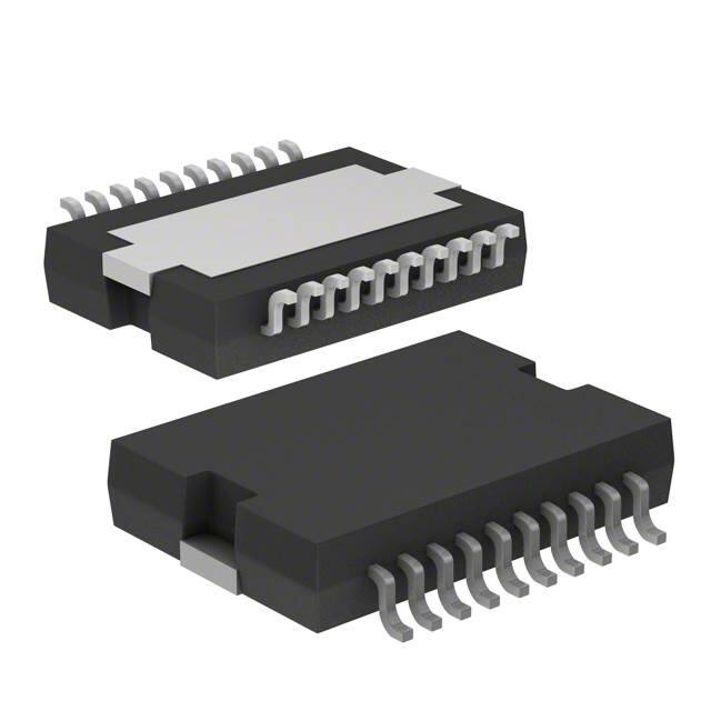
Power SO-20 TM
Built-in thermal shut-down protects the chip from
over temperature and short circuit.
The control inputs are 5V CMOS logic level
compatible.
The open drain diagnostic outputs indicate short
circuit (no load) and overtemperature status.
BLOCK DIAGRAM
SC09570
February 1998
1/9
�VN450
ABSOLUTE MAXIMUM RATING
Symbol
VCC
-V CC
-I gnd
I OUT 1,2
IOUT 3
I R 1,2
IR 3
I IN 1,2,3
I STAT 1,2,3
V ESD
P tot
Tj
T stg
Parameter
Supply Voltage (continuous)
Reverse Supply Voltage (continuous)
Reverse Ground Current
Output Current (continuous), channels 1, 2
Output Current (continuous), channel 3
Reverse Output Current (continuous) channels 1, 2
Reverse Output Current (continuous) channel 3
Input Current
Status Output Current
Electrostatic Discharge (R=1.5 kΩ, C=100 pF)
Power Dissipation at T c ≤ 25 o C
Junction Operating Temperature
Storage Temperature
CONNECTION DIAGRAM
CURRENT AND VOLTAGE CONVENTIONS
2/9
Value
45
-0.3
-200
10
2.5
-10
-2.5
±10
±10
2000
95
-40 to 150
-55 to 150
Unit
V
V
mA
A
A
A
A
mA
mA
V
W
o
C
o
C
�VN450
ELECTRICAL TRANSIENTS REQUIREMENTS
ISO T/R
7637/1
Test Pulse
TEST LEVELS
I
II
III
IV
Delays and
Impedance
1
-25 V
-50 V
-75 V
-100 V
2 ms, 10 Ω
2
+25 V
+50 V
+75 V
+100 V
0.2 ms, 10 Ω
3a
-25 V
-50 V
-100 V
-150 V
0.1 µs, 50 Ω
3b
+25 V
+50 V
+75 V
+100 V
0.1 µs, 50 Ω
4
-4 V
-5 V
-6 V
-7 V
100 ms, 0.01 Ω
5
+26.5 V
+46.5 V
+66.5 V
+86.5 V
400 ms, 2 Ω
ISO T/R
7637/1
Test Pulse
TEST LEVELS RESULTS
I
II
III
IV
1
C
C
C
C
2
C
C
C
C
3a
C
C
C
C
3b
C
C
C
C
4
C
C
C
C
5
C
E
E
E
(With a series resistor ≥ 1 KΩ in input and status pins).
CLASS
CONTENTS
C
All function of the device are performed as designed after exposure to disturbance.
E
One or more functions of the device is not performed as designed after exposure and
cannot be returned to proper operation without replacing the device.
3/9
�VN450
THERMAL DATA
R thj-case
R thj-amb
Thermal Resistance Junction-case (1)
Max
Thermal Resistance Junction-ambient
Max
1.3
o
C/W
50
o
C/W
ELECTRICAL CHARACTERISTICS (VCC = 13 V; -40 oC < Tj < 125 oC unless otherwise specified)
POWER
Symbol
Parameter
VCC
Operating Supply
Voltage
V usd
Under Voltage
Shut-Down
V ov
Overvoltage Shut-Down
R on
IS
On State Resistance
Supply Current
Test Conditions
I OUT
I OUT
I OUT
I OUT
=2A
=2A
= 0.5 A
= 0.5 A
1,2
1,2
3
3
Min.
Typ.
Max.
Unit
5.5
13
36
V
3
4
5.5
V
36
39
45
V
40
75
300
540
mΩ
mΩ
mΩ
mΩ
30
4.2
60
10
µA
mA
Typ.
Max.
Unit
1.5
V
o
T j = 25 C
T j = 25 o C
o
Off state
On state
T case = 25 C
LOGIC INPUT (Channel1,2,3)
Symbol
Parameter
Test Conditions
V IL
Input Low Level
Voltage
(*)
VIH
Input High Level
Voltage (see note 1)
(*)
V I(hyst.)
I IN
V ICL
Min.
3.5
Input Hysteresis
Voltage
0.2
V
0.85
T case = 25 o C
Input Current
V IN = 5 V
Input Clamp Voltage
I IN = 10 mA
I IN = -10 mA
5
6
-0.7
1.5
V
100
µA
7
V
V
(*) : The input voltage is internally clamped at 6 V about. It is possible to connect this pin to an higher voltage via an external resistor
provided the input current does not exceed 10 mA.
SWITCHING (VCC = 13 V; Tj = 25 oC; input rise time < 0.1µs)
Symbol
Parameter
Min.
Typ.
Max.
Unit
t d(on)
Turn-on Delay Time Of
Output Current
R 1 = 6.5 Ω
R 1 = 26 Ω
Channels 1,2
Channels 3
10
2
40
20
140
70
µs
µs
Rise Time Of Output
Current
R 1 = 6.5 Ω
R 1 = 26 Ω
Channels 1,2
Channels 3
32
8
150
20
300
60
µs
µs
Turn-off Delay Time Of
Output Current
R 1 = 6.5 Ω
R 1 = 26 Ω
Channels 1,2
Channels 3
120
30
300
75
600
150
µs
µs
Fall Time Of Output
Current
R 1 = 6.5 Ω
R 1 = 26 Ω
Channels 1,2
Channels 3
32
8
80
20
160
50
µs
µs
di/dt (on)
Turn-on Current Slope
R 1 = 6.5 Ω
R 1 = 26 Ω
Channels 1,2
Channels 3
0.02
0.02
0.05
0.05
A/µs
A/µs
di/dt(of f)
Turn-off Current Slope
R 1 = 6.5 Ω
R 1 = 26 Ω
Channels 1,2
Channels 3
0.02
0.02
0.05
0.05
A/µs
A/µs
tr
t d(off)
tf
4/9
Test Conditions
�VN450
ELECTRICAL CHARACTERISTICS (continued)
PROTECTIONS AND DIAGNOSTICS
Symbol
Min.
Typ.
Max.
T TSD
Thermal Shut-down
Temperature
150
170
190
T TR
Thermal Reset
Temperature
135
T RSD
Parameter
Test Conditions
Thermal Hysteresis
Unit
o
C
o
C
o
C
5
15
30
5.2
6.6
8
V
100
5
450
50
800
100
mA
mA
10
2
18
3.5
A
A
3.4
2
A
A
(HYST)
Output Voltage
Authorizing Openload
Detection
8V ≤ V CC ≤ 36V
I OL
Open Load Current
Level
Channels 1,2
Channels 3
8V ≤ V CC ≤ 18V
8V ≤ V CC ≤ 30V
I OV
Over Current
R 1 ≤10 mΩ
R 1 ≤10 mΩ
channels 1,2
channel 3
I AV
Average Current in
Short Circuit
R 1 ≤10 mΩ
channels 1,2
channel 3
VENOL
T Case =85 o C
V STAT1,2,3 Status Output Voltage
I STAT = 1.6 mA (Fault Condition)
V SCL1,2,3
Status Clamp Voltage
I STAT = 10 mA
I STAT = -10 mA
5.5
t POL
Status Delay
(∗) (see figure 1)
50
t POVL
Status Delay
(∗) (see figure 1)
Turn-off Output Clamp
Voltage
I OUT1 = 2 A
I OUT2 = 2 A
I OUT3 = 0.5 A
V DEMAG
(∗) ISO definitions
L = 1 mH
L = 1 mH
L = 1 mH
V IN1 = 0
V IN2 = 0
V IN3 = 0
0.4
V
6
-0.7
7
V
V
300
950
µs
10
µs
V CC -45 VCC -50 V CC -55
V
TPOL = Status delay in case of open load conditions
TPOVL = Status delay in case of over load conditions
5/9
�VN450
FIGURE 1
SWITCHING PARAMETERS TEST CONDITIONS
TRUTH TABLE (Channels 1,2,3)
INPUT
OUTPUT
STATUS
Normal Operation
Conditions
L
H
L
H
H
H
Over-voltage
X
L
H
Under-voltage
X
L
H
Thermal shut-down
H
L
L
Open load
H
H = high level, L= low level, X= unspecified
H
L
6/9
�VN450
FIGURE 2: Switching Waveforms
7/9
�VN450
PowerSO-20 MECHANICAL DATA
DIM.
mm
TYP.
MIN.
A
a1
a2
a3
b
c
D (1)
E
e
MAX.
3.60
0.30
3.30
0.10
0.53
0.32
16.00
14.50
0.10
0
0.40
0.23
15.80
13.90
inch
TYP.
MIN.
0.0039
0
0.0157
0.009
0.6220
0.5472
1.27
e3
E1 (1)
E2
G
0.050
11.43
0.450
10.90
h
L
N
0
11.10
2.90
0.10
0.80
1.10
1.10
S
T
MAX.
0.1417
0.0118
0.1299
0.0039
0.0209
0.0126
0.6299
0.570
0.4291
0.437
0.1141
0.0039
0
0.0433
0.0433
0.0314
10o (max.)
8o (max.)
10.0
0.3937
(1) "D and E1" do not include mold flash or protusions
- Mold flash or protusions shall not exceed 0.15mm (0.006")
N
R
N
a2
b
DETAIL A
A
e
c
a1
DETAIL B
E
e3
D
DETAIL A
lead
20
11
slug
a3
DETAIL B
E2
E1
0.35
Gage Plane
T
-C-
S
L
SEATING PLANE
G
C
(COPLANARITY)
1
10
PSO20MEC
h x 45°
8/9
0056635
�VN450
Information furnished is believed to be accurate and reliable. However, SGS-THOMSON Microelectronics assumes no responsability for the
consequences of use of such information nor for any infringement of patents or other rights of third parties which may results from its use. No
license is granted by implication or otherwise under any patent or patent rights of SGS-THOMSON Microelectronics. Specifications mentioned
in this publication are subject to change without notice. This publication supersedes and replaces all information previously supplied.
SGS-THOMSON Microelectronics products are not authorized for use as critical components in life support devices or systems without express
written approval of SGS-THOMSON Microelectonics.
© 1998 SGS-THOMSON Microelectronics - Printed in Italy - All Rights Reserved
SGS-THOMSON Microelectronics GROUP OF COMPANIES
Australia - Brazil - Canada - China - France - Germany - Italy - Japan - Korea - Malaysia - Malta - Morocco - The Netherlands Singapore - Spain - Sweden - Switzerland - Taiwan - Thailand - United Kingdom - U.S.A
...
9/9
�
很抱歉,暂时无法提供与“VN450P13TR”相匹配的价格&库存,您可以联系我们找货
免费人工找货- 国内价格 香港价格
- 600+42.95545600+5.55605