VN460SP
SINGLE CHANNEL HIGH SIDE SMART
SOLID STATE RELAY
T YPE
V de ma g
R DS(o n)
IO UT
V CC
VN460SP
V CC -55V
20 m Ω
25 A
36 V
■
■
■
■
■
■
■
OUTPUT CURRENT (CONTINUOUS):
25 A @ TC = 25 o C
5 V LOGIC LEVEL COMPATIBLE INPUT
UNDER VOLTAGE SHUT-DOWN
OVER VOLTAGE SHUT-DOWN
THERMAL SHUT-DOWN
OPEN DRAIN DIAGNOSTIC OUTPUT
VERY LOW STAND-BY POWER
DISSIPATION
u
d
o
1
r
P
e
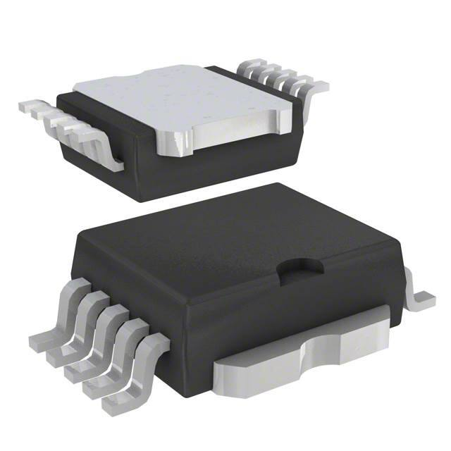
Power SO-10 TM
DESCRIPTION
The VN460SP is a monolithic device made using
SGS-THOMSON Vertical Intelligent Power
Technology, intended for driving resistive or
inductive loads with one side connected to
ground.
Built-in thermal shut-down protects the chip from
over temperature and short circuit.
)-
s
(
t
c
u
d
o
)
s
(
ct
10
t
e
l
o
s
b
O
The control input is 5V CMOS logic level
compatible.
The open drain diagnostic output indicates open
circuit (no load) and overtemperature status.
r
P
e
BLOCK DIAGRAM
t
e
l
o
s
b
O
September 2013
DocID5691 Rev 3
1/9
�VN460SP
ABSOLUTE MAXIMUM RATING
Symb ol
Parameter
VCC
Power Supply Voltage (continuous)
-V CC
Reverse Supply Voltage (continuous)
I OUT
Output Current (continuous)
Unit
45
V
-0.3
V
Internally Limited
A
IR
Reverse Output Current
-25
A
I IN
Input Current
±10
mA
I STAT
Status Pin Current
±10
mA
-I GND
Reverse Ground Current
-200
mA
V ESD
Electrostatic Discharge (1.5 kΩ, 100 pF)
2000
V
o
P tot
Power Dissipation at T c ≤ 25 C
112
Tj
Junction Operating Temperature
-40 to 150
Storage Temperature
-55 to 150
T s tg
r
P
e
t
e
l
o
)
(s
t
c
u
d
o
r
P
e
t
e
l
o
CURRENT AND VOLTAGE CONVENTIONS
s
b
O
)
s
(
ct
u
d
o
CONNECTION DIAGRAM
2/9
Value
s
b
O
W
o
C
o
C
�VN460SP
ELECTRICAL TRANSIENTS REQUIREMENTS
ISO T/R
7637/1
Test Pu lse
T EST LEVEL S
I
II
III
IV
Delays an d
Impedance
1
-25 V
-50 V
-75 V
-100 V
2 ms, 10 Ω
2
+25 V
+50 V
+75 V
+100 V
0.2 ms, 10 Ω
3a
-25 V
-50 V
-100 V
-150 V
0.1 µs, 50 Ω
+50 V
+75 V
+100 V
0.1 µs, 50 Ω
3b
+25 V
4
-4 V
-5 V
-6 V
-7 V
100 ms, 0.01 Ω
5
+26.5
+46.5
+66.5
+86.5
400 ms, 2 Ω
ISO T/R
7637/1
Test Pu lse
TEST L EVELS RESUL TS
I
II
III
1
C
C
C
2
C
C
C
3a
C
C
3b
C
C
4
C
C
5
C
(s)
E
(With a series resistor ≥ 1 KΩ in input and status pins).
od
CL ASS
r
P
e
C
t
e
l
o
E
t
c
u
C
-O
u
d
o
r
P
e
IV
let
o
s
b
)
s
(
ct
C
C
C
C
C
C
C
E
E
CONT ENT S
All function of the device are performed as designed after exposure to disturbance.
One or more functions of the device is not performed as designed after exposure and
cannot be returned to proper operation without replacing the device.
s
b
O
3/9
�VN460SP
THERMAL DATA
R t hj-ca se
R thj-a (∗)
Thermal Resistance Junction-case
Max
Thermal Resistance Junction-ambient
Max
1.1
o
C/W
50
o
C/W
(∗) When mounted using minimum recommended pad size on FR-4 board.
ELECTRICAL CHARACTERISTICS (VCC = 13 V; -40 oC < TJ < 125 oC unless otherwise specified)
POWER
Symb ol
Parameter
VCC
Operating Supply
Voltage
V usd
Under Voltage Shut
Down
V ov
Overvoltage Shut Down
R on
IS
Test Cond ition s
On State Resistance
I OUT = 5 A
I OUT = 5 A
T J = 25 C
Supply Current
Off state
On State
TCase = 25 C
t
e
l
o
Input Low Level
Voltage
(*)
VI H
Input High Level
Voltage (see note 1)
(*)
V I(hyst.)
Input Hysteresis
Voltage
V ICL
Pr
Input Clamp Voltage
e
t
e
ol
O
)
s
(
t
c
u
d
o
Input Current
I IN
bs
Test Cond ition s
VI L
Max.
Un it
13
36
V
3
4
36
39
Min.
V
45
V
20
36
mΩ
mΩ
15
1.4
30
3.3
µA
mA
Typ .
Max.
Un it
1.5
V
3.5
0.2
V
0.85
Tc ase = 25 oC
VI N = 5 V
I IN = 10 mA
I IN = -10 mA
)
s
(
ct
5.5
u
d
o
r
P
e
o
Parameter
Typ .
5.5
o
LOGIC INPUT
Symb ol
Min.
5
6
-0.7
1.5
V
100
µA
7
V
V
(*) : The input voltage is internally clamped at 6 V about. It is possible to connect this pin to an higher voltage via an external resistor
provided the input current does not exceed 10 mA.
SWITCHING (VCC = 13 V)
s
b
O
Symb ol
Parameter
Test Cond ition s
Min.
Typ .
Max.
Un it
t d(on)
Turn-on Delay Time Of
Output Current
I OUT = 5 A
Resistive Load
Input Rise T ime < 0.1 µs T j = 25 o C
25
90
250
µs
Rise Time O f O utput
Current
I OUT = 5 A
Resistive Load
Input Rise T ime < 0.1 µs T j = 25 o C
80
300
650
µs
Turn-off Delay Time O f I OUT = 5 A
Resistive Load
Output Current
Input Rise T ime < 0.1 µs T j = 25 o C
300
750
1500
µs
Fall T ime Of Output
Current
I OUT = 5 A
Resistive Load
o
Input Rise T ime < 0.1 µs T j = 25 C
80
200
400
µs
(di/dt) on
Turn-on Current Slope
I OUT = 5 A
0.02
0.05
A/µs
(di/dt) off
Turn-off Current Slope
I OUT = 5 A
0.02
0.05
A/µs
tr
t d(of f)
tf
4/9
�VN460SP
ELECTRICAL CHARACTERISTICS (continued)
PROTECTIONS AND DIAGNOSTICS
Symb ol
Min.
Typ .
Max.
T TSD
Thermal Shut-down
Temperature
Parameter
Test Cond ition s
150
170
190
T TR
Thermal Reset
Temperature
135
T RSD
Thermal Hysteresis
5
15
50
Un it
o
C
o
C
o
C
(HYST)
Output Voltage
Authorizing Openload
Detection
8V≤VCC ≤30V
5.2
6.6
8
I OL
Open Load Current
Level
8V≤VCC ≤30V
100
800
1500
I OV
Over Current
R LOAD ≤10 mΩ
o
o
- 40 C
很抱歉,暂时无法提供与“VN460SP”相匹配的价格&库存,您可以联系我们找货
免费人工找货- 国内价格 香港价格
- 500+37.50072500+4.85172