VN5012AK-E
Single channel high side driver with analog current sense
for automotive applications
Datasheet − production data
Features
Max supply voltage
VCC
41 V
Operating voltage range
VCC
4.5 to 36 V
Max on-state resistance (per ch.)
RON
12 mΩ
Current limitation (typ)
ILIMH
65 A
IS
2 µA(1)
Off-state supply current (typ)
1.
Typical value with all loads connected
■
General features
– Inrush current active management by
power limitation
– Very low stand-by current
– 3.0 V CMOS compatible input
– Optimized electromagnetic emission
– Very low electromagnetic susceptibility
– In compliance with the 2002/95/EC
european directive
– Reverse battery protection
– Electrostatic discharge protection
Application
■
All types of resistive, inductive and capacitive
loads
Description
■
Diagnostic functions
– Proportional load current sense
– High current sense precision for wide range
currents
– Current sense disable
– Thermal shutdown indication
– Very low current sense leakage
■
Protections
– Undervoltage shutdown
– Overvoltage clamp
– Load current limitation
– Self limiting of fast thermal transients
– Protection against loss of ground and loss
of VCC
– Thermal shutdown
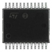
Table 1.
PowerSSO-24
The VN5012AK-E is a monolithic device made
using STMicroelectronics VIPower® M0-5
technology. It is intended for driving resistive or
inductive loads with one side connected to
ground. Active VCC pin voltage clamp protects the
device against low energy spikes (see ISO7637
transient compatibility table). This device
integrates an analog current sense which delivers
a current proportional to the load current
(according to a known ratio) when CS_DIS is
driven low or left open. When CS_DIS is driven
high, the CURRENT SENSE pin is in a high
impedance condition. Output current limitation
protects the device in overload condition. In case
of long overload duration, the device limits the
dissipated power to safe level up to thermal
shutdown intervention. Thermal shutdown with
automatic restart allows the device to recover
normal operation as soon as fault condition
disappears.
Device summary
Order codes
Package
PowerSSO-24
September 2013
This is information on a product in full production.
Tube
Tape and reel
VN5012AK-E
VN5012AKTR-E
Doc ID 13240 Rev 9
1/30
www.st.com
1
�Contents
VN5012AK-E
Contents
1
Block diagram and pin description . . . . . . . . . . . . . . . . . . . . . . . . . . . . . 5
2
Electrical specifications . . . . . . . . . . . . . . . . . . . . . . . . . . . . . . . . . . . . . . 7
3
2.1
Absolute maximum ratings . . . . . . . . . . . . . . . . . . . . . . . . . . . . . . . . . . . . . 7
2.2
Thermal data . . . . . . . . . . . . . . . . . . . . . . . . . . . . . . . . . . . . . . . . . . . . . . . 8
2.3
Electrical characteristics . . . . . . . . . . . . . . . . . . . . . . . . . . . . . . . . . . . . . . . 8
2.4
Electrical characteristics curves . . . . . . . . . . . . . . . . . . . . . . . . . . . . . . . . 17
Application information . . . . . . . . . . . . . . . . . . . . . . . . . . . . . . . . . . . . . 20
3.1
4
6
2/30
3.1.1
Solution 1: resistor in the ground line (RGND only) . . . . . . . . . . . . . . . . 20
3.1.2
Solution 2: a diode (DGND) in the ground line . . . . . . . . . . . . . . . . . . . 21
3.2
Load dump protection . . . . . . . . . . . . . . . . . . . . . . . . . . . . . . . . . . . . . . . . 21
3.3
MCU I/Os protection . . . . . . . . . . . . . . . . . . . . . . . . . . . . . . . . . . . . . . . . . 21
3.4
Maximum demagnetization energy (VCC = 13.5V) . . . . . . . . . . . . . . . . . 22
Package and PCB thermal data . . . . . . . . . . . . . . . . . . . . . . . . . . . . . . . 23
4.1
5
GND Protection network against reverse battery . . . . . . . . . . . . . . . . . . . 20
PowerSSO-24 thermal data . . . . . . . . . . . . . . . . . . . . . . . . . . . . . . . . . . . 23
Package and packing information . . . . . . . . . . . . . . . . . . . . . . . . . . . . . 26
5.1
ECOPACK® packages . . . . . . . . . . . . . . . . . . . . . . . . . . . . . . . . . . . . . . . 26
5.2
PowerSSO-24 package mechanical data . . . . . . . . . . . . . . . . . . . . . . . . . 26
5.3
PowerSSO-24 packing information . . . . . . . . . . . . . . . . . . . . . . . . . . . . . 28
Revision history . . . . . . . . . . . . . . . . . . . . . . . . . . . . . . . . . . . . . . . . . . . 29
Doc ID 13240 Rev 9
�VN5012AK-E
List of tables
List of tables
Table 1.
Table 2.
Table 3.
Table 4.
Table 5.
Table 6.
Table 7.
Table 8.
Table 9.
Table 10.
Table 11.
Table 12.
Table 13.
Table 14.
Table 15.
Table 16.
Table 17.
Device summary . . . . . . . . . . . . . . . . . . . . . . . . . . . . . . . . . . . . . . . . . . . . . . . . . . . . . . . . . . 1
Pin function . . . . . . . . . . . . . . . . . . . . . . . . . . . . . . . . . . . . . . . . . . . . . . . . . . . . . . . . . . . . . . 5
Suggested connections for unused and not connected pins . . . . . . . . . . . . . . . . . . . . . . . . 6
Absolute maximum ratings . . . . . . . . . . . . . . . . . . . . . . . . . . . . . . . . . . . . . . . . . . . . . . . . . . 7
Thermal data. . . . . . . . . . . . . . . . . . . . . . . . . . . . . . . . . . . . . . . . . . . . . . . . . . . . . . . . . . . . . 8
Power section . . . . . . . . . . . . . . . . . . . . . . . . . . . . . . . . . . . . . . . . . . . . . . . . . . . . . . . . . . . . 8
Switching (VCC = 13 V; Tj = 25°C) . . . . . . . . . . . . . . . . . . . . . . . . . . . . . . . . . . . . . . . . . . . . 9
Logic input . . . . . . . . . . . . . . . . . . . . . . . . . . . . . . . . . . . . . . . . . . . . . . . . . . . . . . . . . . . . . . 9
Protections and diagnostics . . . . . . . . . . . . . . . . . . . . . . . . . . . . . . . . . . . . . . . . . . . . . . . . 10
Current sense (8 V < VCC < 16 V). . . . . . . . . . . . . . . . . . . . . . . . . . . . . . . . . . . . . . . . . . . . 10
Truth table. . . . . . . . . . . . . . . . . . . . . . . . . . . . . . . . . . . . . . . . . . . . . . . . . . . . . . . . . . . . . . 14
Electrical transient requirements (part 1/3) . . . . . . . . . . . . . . . . . . . . . . . . . . . . . . . . . . . . . 15
Electrical transient requirements (part 2/3) . . . . . . . . . . . . . . . . . . . . . . . . . . . . . . . . . . . . . 15
Electrical transient requirements (part 3/3) . . . . . . . . . . . . . . . . . . . . . . . . . . . . . . . . . . . . . 15
Thermal parameter . . . . . . . . . . . . . . . . . . . . . . . . . . . . . . . . . . . . . . . . . . . . . . . . . . . . . . . 25
PowerSSO-24 mechanical data . . . . . . . . . . . . . . . . . . . . . . . . . . . . . . . . . . . . . . . . . . . . . 27
Document revision history . . . . . . . . . . . . . . . . . . . . . . . . . . . . . . . . . . . . . . . . . . . . . . . . . 29
Doc ID 13240 Rev 9
3/30
�List of figures
VN5012AK-E
List of figures
Figure 1.
Figure 2.
Figure 3.
Figure 4.
Figure 5.
Figure 6.
Figure 7.
Figure 8.
Figure 9.
Figure 10.
Figure 11.
Figure 12.
Figure 13.
Figure 14.
Figure 15.
Figure 16.
Figure 17.
Figure 18.
Figure 19.
Figure 20.
Figure 21.
Figure 22.
Figure 23.
Figure 24.
Figure 25.
Figure 26.
Figure 27.
Figure 28.
Figure 29.
Figure 30.
Figure 31.
Figure 32.
Figure 33.
Figure 34.
4/30
Block diagram . . . . . . . . . . . . . . . . . . . . . . . . . . . . . . . . . . . . . . . . . . . . . . . . . . . . . . . . . . . . 5
Configuration diagram (top view) . . . . . . . . . . . . . . . . . . . . . . . . . . . . . . . . . . . . . . . . . . . . . 6
Current and voltage conventions . . . . . . . . . . . . . . . . . . . . . . . . . . . . . . . . . . . . . . . . . . . . . 7
Current sense delay characteristics . . . . . . . . . . . . . . . . . . . . . . . . . . . . . . . . . . . . . . . . . . 12
Delay response time between rising edge of output current and rising edge of current
sense (CS enabled) . . . . . . . . . . . . . . . . . . . . . . . . . . . . . . . . . . . . . . . . . . . . . . . . . . . . . . 12
IOUT/ISENSE vs IOUT . . . . . . . . . . . . . . . . . . . . . . . . . . . . . . . . . . . . . . . . . . . . . . . . . . . . . . 13
Maximum current sense ratio drift vs load current . . . . . . . . . . . . . . . . . . . . . . . . . . . . . . . 13
Switching characteristics . . . . . . . . . . . . . . . . . . . . . . . . . . . . . . . . . . . . . . . . . . . . . . . . . . 14
Output voltage drop limitation . . . . . . . . . . . . . . . . . . . . . . . . . . . . . . . . . . . . . . . . . . . . . . . 14
Waveforms . . . . . . . . . . . . . . . . . . . . . . . . . . . . . . . . . . . . . . . . . . . . . . . . . . . . . . . . . . . . . 16
Off-state output current. . . . . . . . . . . . . . . . . . . . . . . . . . . . . . . . . . . . . . . . . . . . . . . . . . . . 17
High level input current . . . . . . . . . . . . . . . . . . . . . . . . . . . . . . . . . . . . . . . . . . . . . . . . . . . . 17
Input clamp voltage. . . . . . . . . . . . . . . . . . . . . . . . . . . . . . . . . . . . . . . . . . . . . . . . . . . . . . . 17
Input high level . . . . . . . . . . . . . . . . . . . . . . . . . . . . . . . . . . . . . . . . . . . . . . . . . . . . . . . . . . 17
Input low level . . . . . . . . . . . . . . . . . . . . . . . . . . . . . . . . . . . . . . . . . . . . . . . . . . . . . . . . . . . 17
Input hysteresis voltage . . . . . . . . . . . . . . . . . . . . . . . . . . . . . . . . . . . . . . . . . . . . . . . . . . . 17
On-state resistance vs Tcase . . . . . . . . . . . . . . . . . . . . . . . . . . . . . . . . . . . . . . . . . . . . . . . . 18
On-state resistance vs VCC. . . . . . . . . . . . . . . . . . . . . . . . . . . . . . . . . . . . . . . . . . . . . . . . . 18
Undervoltage shutdown . . . . . . . . . . . . . . . . . . . . . . . . . . . . . . . . . . . . . . . . . . . . . . . . . . . 18
ILIMH vs Tcase . . . . . . . . . . . . . . . . . . . . . . . . . . . . . . . . . . . . . . . . . . . . . . . . . . . . . . . . . . . 18
Turn-on voltage slope . . . . . . . . . . . . . . . . . . . . . . . . . . . . . . . . . . . . . . . . . . . . . . . . . . . . . 18
Turn-off voltage slope . . . . . . . . . . . . . . . . . . . . . . . . . . . . . . . . . . . . . . . . . . . . . . . . . . . . . 18
CS_DIS high level voltage . . . . . . . . . . . . . . . . . . . . . . . . . . . . . . . . . . . . . . . . . . . . . . . . . 19
CS_DIS clamp voltage . . . . . . . . . . . . . . . . . . . . . . . . . . . . . . . . . . . . . . . . . . . . . . . . . . . . 19
CS_DIS low level voltage . . . . . . . . . . . . . . . . . . . . . . . . . . . . . . . . . . . . . . . . . . . . . . . . . . 19
Application schematic . . . . . . . . . . . . . . . . . . . . . . . . . . . . . . . . . . . . . . . . . . . . . . . . . . . . . 20
Maximum turn-off current versus inductance . . . . . . . . . . . . . . . . . . . . . . . . . . . . . . . . . . . 22
PowerSSO-24 PC board. . . . . . . . . . . . . . . . . . . . . . . . . . . . . . . . . . . . . . . . . . . . . . . . . . . 23
Rthj-amb vs PCB copper area in open box free air condition . . . . . . . . . . . . . . . . . . . . . . 23
Rthj-amb vs PCB copper area in open box free air condition . . . . . . . . . . . . . . . . . . . . . . 24
Thermal fitting model of a single channel HSD in PowerSSO-24 . . . . . . . . . . . . . . . . . . . 24
PowerSSO-24 package dimensions . . . . . . . . . . . . . . . . . . . . . . . . . . . . . . . . . . . . . . . . . . 26
PowerSSO-24 tube shipment (no suffix) . . . . . . . . . . . . . . . . . . . . . . . . . . . . . . . . . . . . . . 28
PowerSSO-24 tape and reel shipment (suffix “TR”) . . . . . . . . . . . . . . . . . . . . . . . . . . . . . . 28
Doc ID 13240 Rev 9
�VN5012AK-E
1
Block diagram and pin description
Block diagram and pin description
Figure 1.
Block diagram
VCC
VCC
CLAMP
UNDERVOLTAGE
PwCLAMP
DRIVER
OUTPUT
GND
ILIM
LOGIC
VDSLIM
PwrLIM
INPUT
OVERTEMP.
IOUT
K
CURRENT
SENSE
CS_DIS
Table 2.
Pin function
Name
VCC
OUTPUT
GND
INPUT
CURRENT
SENSE1,2
CS_DIS
Function
Battery connection.
Power output.
Ground connection. Must be reverse battery protected by an external diode/resistor
network.
Voltage controlled input pin with hysteresis, CMOS compatible. Controls output
switch state.
Analog current sense pin, delivers a current proportional to the load current.
Active high CMOS compatible pin, to disable the current sense pin.
Doc ID 13240 Rev 9
5/30
�Block diagram and pin description
Figure 2.
VN5012AK-E
Configuration diagram (top view)
VCC
GND
NC
NC
INPUT
NC
CURRENT SENSE
NC
CS_DIS
NC
NC
VCC
1
2
3
4
5
6
7
8
9
10
11
12
24
23
22
21
20
19
18
17
16
15
14
13
NC
NC
NC
OUTPUT
OUTPUT
OUTPUT
OUTPUT
OUTPUT
OUTPUT
NC
NC
NC
TAB = VCC
Table 3.
Suggested connections for unused and not connected pins
Connection / Pin
Current Sense
N.C.
Output
Input
CS_DIS
Floating
N.R.(1)
X
X
X
X
To ground
Through 1 KΩ
resistor
X
N.R.
Through 10 KΩ
resistor
Through 10 KΩ
resistor
1. Not recommended.
6/30
Doc ID 13240 Rev 9
�VN5012AK-E
2
Electrical specifications
Electrical specifications
Figure 3.
Current and voltage conventions
IS
VCC
VF
VCC
IOUT
ICSD
OUTPUT
CS_DIS
VOUT
VCSD
IIN
INPUT
ISENSE
CURRENT SENSE
VSENSE
VIN
GND
IGND
Note:
VF = VOUT - VCC during reverse battery condition.
2.1
Absolute maximum ratings
Stressing the device above the rating listed in Table 4 may cause permanent damage to the
device. These are stress ratings only and operation of the device at these or any other
conditions above those indicated in the Operating sections of this specification is not
implied. Exposure to the conditions in table below for extended periods may affect device
reliability.
Table 4.
Absolute maximum ratings
Symbol
Parameter
Value
Unit
VCC
DC supply voltage
41
V
-VCC
Reverse DC supply voltage
0.3
V
-IGND
DC reverse ground pin current
200
mA
IOUT
DC output current
Internally limited
A
-IOUT
Reverse DC output current
-30
A
DC input current
-1 to 10
mA
DC current sense disable input current
-1 to 10
mA
200
mA
VCC-41
+VCC
V
V
IIN
ICSD
-ICSENSE DC reverse CS pin current
VCSENSE Current sense maximum voltage
Doc ID 13240 Rev 9
7/30
�Electrical specifications
Table 4.
VN5012AK-E
Absolute maximum ratings (continued)
Symbol
Value
Unit
EMAX
Maximum switching energy
(L = 1.25 mH; RL = 0 Ω; Vbat = 13.5 V; Tjstart = 150 °C;
IOUT = IlimL(typ.))
508
mJ
VESD
Electrostatic discharge
(Human Body Model: R = 1.5 KΩ; C = 100 pF)
– INPUT
– CURRENT SENSE
– CS_DIS
– OUTPUT
– VCC
4000
2000
4000
2000
4000
5000
5000
V
V
V
V
V
V
V
VESD
Charge device model (CDM-AEC-Q100-011)
750
V
Junction operating temperature
-40 to 150
°C
Storage temperature
-55 to 150
°C
Tj
Tstg
2.2
Parameter
Thermal data
Table 5.
Thermal data
Symbol
Parameter
Max value
Unit
0.4
°C/W
See Figure 29
°C/W
Rthj-case Thermal resistance junction case (max) (with one channel on)
Rthj-amb
2.3
Thermal resistance junction ambient (max)
Electrical characteristics
8 V < VCC < 36 V; -40°C < Tj < 150°C, unless otherwise specified.
Table 6.
Power section
Symbol
Parameter
VCC
Operating supply voltage
VUSD
VUSDhyst
RON
Vclamp
8/30
Test conditions
Min. Typ. Max. Unit
13
36
V
Undervoltage shutdown
3.5
4.5
V
Undervoltage shutdown
hysteresis
0.5
On-state
resistance(2)
Clamp voltage
4.5
V
IOUT = 5 A; Tj = 25 °C
12
mΩ
IOUT = 5 A; Tj = 150 °C
24
mΩ
IOUT = 5 A; VCC = 5 V; Tj = 25 °C
16
mΩ
52
V
IS = 20 mA
Doc ID 13240 Rev 9
41
46
�VN5012AK-E
Electrical specifications
Table 6.
Power section (continued)
Symbol
IS
IL(off)
VF
Parameter
Test conditions
Supply current
Off-state output current(2)
Output - VCC diode
voltage(2)
Min. Typ. Max. Unit
Off-state; VCC = 13 V; Tj = 25 °C;
VIN = VOUT = VSENSE = VCSD = 0 V
2(1)
5(1)
µA
On-state; VCC = 13 V; VIN = 5 V;
IOUT = 0 A
1.5
3
μΑ
0.01
3
µA
5
µA
0.7
V
VIN = VOUT = 0 V; VCC = 13 V;
Tj = 25 °C
0
VIN = VOUT = 0 V; VCC = 13 V;
Tj = 125 °C
0
-IOUT = 8 A; Tj = 150 °C
1. PowerMOS leakage included.
2. For each channel.
Table 7.
Symbol
Switching (VCC = 13 V; Tj = 25°C)
Parameter
Test conditions
Min.
Typ.
Max.
Unit
td(on)
Turn-on delay time
RL = 2.6 Ω (see Figure 8)
30
µs
td(off)
Turn-off delay time
RL = 2.6 Ω (see Figure 8)
55
µs
dVOUT/dt(on)
Turn-on voltage slope
RL = 2.6 Ω
See Figure 21
V/µs
dVOUT/dt(off)
Turn-off voltage slope
RL = 2.6 Ω
See Figure 22
V/µs
WON
Switching energy losses
during twon
RL = 2.6 Ω (see Figure 8)
1.2
mJ
WOFF
Switching energy losses
during twoff
RL = 2.6 Ω (see Figure 8)
0.7
mJ
Table 8.
Symbol
Logic input
Parameter
VIL
Input low level voltage
IIL
Low level input current
VIH
Input high level voltage
IIH
High level input current
VI(hyst)
Input hysteresis voltage
VICL
Test conditions
VIN = 0.9 V
CS_DIS low level voltage
ICSDL
Low level CS_DIS current
VCSDH
CS_DIS high level voltage
ICSDH
High level CS_DIS current
Max.
Unit
0.9
V
1
µA
2.1
V
10
0.25
7
-0.7
VCSD = 2.1 V
Doc ID 13240 Rev 9
V
V
0.9
VCSD = 0.9 V
µA
V
5.5
IIN = -1 mA
VCSDL
Typ.
VIN = 2.1 V
IIN = 1 mA
Input clamp voltage
Min.
V
1
µA
2.1
V
10
µA
9/30
�Electrical specifications
Table 8.
Symbol
VN5012AK-E
Logic input (continued)
Parameter
Test conditions
Min.
VCSD(hyst) CS_DIS hysteresis voltage
VCSCL
Table 9.
Symbol
CS_DIS clamp voltage
Parameter
V
5.5
7
-0.7
Test conditions
IlimL
Short circuit current
during thermal cycling
TTSD
Shutdown temperature
V
V
VCC = 13 V
Min.
Typ.
Max.
Unit
45
65
90
A
90
A
5 V < VCC < 36 V
VCC = 13 V;
TR < Tj < TTSD
TR
Reset temperature
TRS
Thermal reset of STATUS
VON
ICSD = 1 mA
Unit
Protections and diagnostics (1)
DC Short circuit current
VDEMAG
Max.
0.25
ICSD = -1 mA
IlimH
THYST
Typ.
24
150
175
TRS + 1
TRS + 5
A
200
°C
135
Thermal hysteresis
(TTSD - TR)
°C
°C
7
°C
Turn-off output voltage
clamp
IOUT = 2 A; VIN = 0 V;
L = 6 mH
VCC - 41 VCC - 46 VCC - 52
V
Output voltage drop
limitation
IOUT = 0.5 A;
Tj = -40 °C to 150 °C
(see Figure 9)
25
mV
1. To ensure long term reliability under heavy overload or short circuit conditions, protection and related
diagnostic signals must be used together with a proper software strategy. If the device is subjected to
abnormal conditions, this software must limit the duration and number of activation cycles.
Table 10.
Symbol
K0
K1
dK1/K1(1)
K2
dK2/K2(1)
10/30
Current sense (8 V < VCC < 16 V)
Parameter
Test conditions
Min. Typ. Max. Unit
IOUT/ISENSE
IOUT = 0.25 A; VSENSE = 0.5 V;
VCSD = 0 V; Tj = -40 °C to 150 °C
IOUT/ISENSE
IOUT = 5 A; VSENSE = 0.5 V; VCSD = 0 V;
3590 4480 5370
Tj = -40 °C to 150 °C
IOUT = 5 A; VSENSE = 0.5 V; VCSD = 0 V;
3790 4480 5170
Tj = 25 °C to 150 °C
Current sense ratio
drift
IOUT = 5 A; VSENSE = 0.5 V; VCSD = 0 V;
Tj = -40 °C to 150 °C
IOUT/ISENSE
IOUT = 10 A; VSENSE = 4 V; VCSD = 0 V;
Tj = -40 °C to 150 °C
IOUT = 10 A; VSENSE = 4 V; VCSD = 0 V;
Tj = 25 °C to 150 °C
Current sense ratio
drift
IOUT = 10 A; VSENSE = 4 V; VCSD = 0 V;
TJ = -40 °C to 150 °C
Doc ID 13240 Rev 9
3090 5080 7070
-8
+8
%
4080 4510 4980
4160 4510 4860
-5
+5
%
�VN5012AK-E
Electrical specifications
Table 10.
Symbol
K3
dK3/K3(1)
ISENSE0
Current sense (8 V < VCC < 16 V) (continued)
Parameter
IOUT/ISENSE
Current sense ratio
drift
Analog sense
leakage current
Test conditions
IOUT = 25 A; VSENSE = 4 V; VCSD = 0 V;
Tj = -40 °C to 150 °C
IOUT = 25 A; VSENSE = 4 V; VCSD = 0 V;
Tj = 25 °C to 150 °C
Min. Typ. Max. Unit
4420 4600 4780
4460 4600 4740
IOUT = 25 A; VSENSE = 4 V; VCSD = 0 V;
Tj = -40 °C to 150 °C
-4
+4
%
IOUT = 0 A; VSENSE = 0 V; VCSD = 5 V;
VIN = 0 V; Tj = -40 °C to 150 °C
0
1
µA
IOUT = 0 A; VSENSE = 0 V; VCSD = 0 V;
VIN = 5 V; Tj = -40 °C to 150 °C
0
2
µA
IOUT = 2 A; VSENSE = 0 V; VCSD = 5 V;
VIN = 5 V; Tj = -40 °C to 150 °C
0
1
µA
45
mA
IOL
Openload on-state
current detection
threshold
VIN = 5 V; ISENSE = 5 µA
10
VSENSE
Max analog sense
output voltage
IOUT = 15 A; VCSD = 0 V
5
Analog sense output
voltage in over
VSENSEH
VCC = 13 V; RSENSE = 2.2 KΩ
temperature
condition
ISENSEH
Analog sense output
current in over
VCC = 13 V; VSENSE = 5 V
temperature
condition
V
9
V
8
mA
Delay response time VSENSE < 4 V; 1.5 A < IOUT < 25 A;
tDSENSE1H from falling edge of ISENSE = 90 % of ISENSE max
(see Figure 4)
CS_DIS pin
50
100
µs
Delay response time VSENSE < 4 V; 1.5 A < IOUT < 25 A;
tDSENSE1L from rising edge of
ISENSE = 10 % of ISENSE max
(see Figure 4)
CS_DIS pin
5
20
µs
Delay response time VSENSE < 4 V; 1.5 A < IOUT < 25 A;
tDSENSE2H from rising edge of
ISENSE = 90 % of ISENSE max
(see Figure 4)
INPUT pin
270
400
µs
300
µs
250
µs
Delay response time
between rising edge
ΔtDSENSE2H of output current and
rising edge of
current sense
VSENSE < 4 V;
ISENSE = 90 % of ISENSEMAX;
IOUT = 90 % of IOUTMAX;
IOUTMAX = 5 A (see Figure 5)
Delay response time VSENSE < 4 V; 1.5 A < IOUT < 25 A;
tDSENSE2L from falling edge of ISENSE = 10 % of ISENSE max
INPUT pin
(see Figure 4)
100
1. Parameter guaranteed by design, it is not tested.
Doc ID 13240 Rev 9
11/30
�Electrical specifications
Figure 4.
VN5012AK-E
Current sense delay characteristics
INPUT
CS_DIS
LOAD CURRENT
SENSE CURRENT
tDSENSE2H
Figure 5.
tDSENSE1L
tDSENSE1H
tDSENSE2L
Delay response time between rising edge of output current and rising
edge of current sense (CS enabled)
VIN
ΔtDSENSE2H
t
IOUT
IOUTMAX
90% IOUTMAX
t
ISENSE
ISENSEMAX
90% ISENSEMAX
t
12/30
Doc ID 13240 Rev 9
�VN5012AK-E
Electrical specifications
Figure 6.
IOUT/ISENSE vs IOUT
,287�,6(16(
����
PD[�7M� ����&�WR����&
����
PD[�7M ���&�WR����&
W\SLFDO�YDOXH
����
PLQ�7M ���&�WR����&
����
PLQ�7M ����&�WR����&
����
����
�
��
��
��
��
,287��$�
Figure 7.
*$3*&)7�����
Maximum current sense ratio drift vs load current
EL�L �
��
��
�
�
��
���
���
�
Note:
��
��
,287��$�
��
��
*$3*&)7�����
Parameter guaranteed by design; it is not tested.
Doc ID 13240 Rev 9
13/30
�Electrical specifications
Table 11.
VN5012AK-E
Truth table
Input
Output
Sense (VCSD = 0 V)(1)
Normal operation
L
H
L
H
0
Nominal
Over temperature
L
H
L
L
0
VSENSEH
Undervoltage
L
H
L
L
0
0
Short circuit to GND
(Rsc ≤ 10 mΩ)
L
H
H
L
L
L
0
0 if Tj < TTSD
VSENSEH if Tj > TTSD
Short circuit to VCC
L
H
H
H
0
< Nominal
Negative output voltage
clamp
L
L
0
Conditions
1. If the VCSD is high, the SENSE output is at a high impedance, its potential depends on leakage currents
and external circuit.
Figure 8.
Switching characteristics
VOUT
tWon
tWoff
90%
80%
dVOUT/dt(off)
dVOUT/dt(on)
10%
tr
tf
t
INPUT
td(on)
td(off)
t
Figure 9.
Output voltage drop limitation
Vcc-Vout
Tj=150oC
Tj=25oC
Tj=-40oC
Von
Von/Ron(T)
14/30
Doc ID 13240 Rev 9
Iout
�VN5012AK-E
Electrical specifications
Table 12.
ISO 7637-2:
2004(E)
Electrical transient requirements (part 1/3)
Test levels(1)
Number of
pulses or
test times
Burst cycle/pulse
repetition time
Delays and
impedance
test pulse
III
IV
1
-75V
-100V
5000
pulses
0.5 s
5s
2 ms, 10 Ω
2a
+37V
+50V
5000
pulses
0.2 s
5s
50 µs, 2 Ω
3a
-100V
-150V
1h
90 ms
100 ms
0.1 µs, 50 Ω
3b
+75V
+100V
1h
90 ms
100 ms
0.1 µs, 50 Ω
4
-6V
-7V
1 pulse
100 ms, 0.01 Ω
5b(2)
+65V
+87V
1 pulse
400 ms, 2 Ω
Table 13.
Electrical transient requirements (part 2/3)
Test level results(1)
ISO 7637-2:
2004(E)
test pulse
III
IV
1
C
C
2
C
C
3a
C
C
3b
C
C
4
C
C
5(2)
C
C
1. The above test levels must be considered referred to VCC = 13.5 V except for pulse 5b.
2.
Valid in case of external load dump clamp: 40V maximum referred to ground.
Table 14.
Electrical transient requirements (part 3/3)
Class
Contents
C
All functions of the device are performed as designed after exposure to disturbance.
E
One or more functions of the device are not performed as designed after exposure
to disturbance and cannot be returned to proper operation without replacing the
Doc ID 13240 Rev 9
15/30
�Electrical specifications
VN5012AK-E
Figure 10. Waveforms
NORMAL OPERATION
INPUT
CS_DIS
LOAD CURRENT
SENSE CURRENT
UNDERVOLTAGE
VUSDhyst
VCC
VUSD
INPUT
CS_DIS
LOAD CURRENT
SENSE CURRENT
SHORT TO VCC
INPUT
CS_DIS
LOAD VOLTAGE
LOAD CURRENT
SENSE CURRENT
很抱歉,暂时无法提供与“VN5012AK-E”相匹配的价格&库存,您可以联系我们找货
免费人工找货- 国内价格 香港价格
- 1225+16.464901225+2.12125