VN5050J-E
Single channel high side driver for automotive applications
Features
General
Max supply voltage Operating voltage range Max On-State resistance Current limitation (typ) Off state supply current (TYP) VCC VCC RON ILIMH IS 41V 4.5 to 36V 50 mΩ 19A 2 µA
■ ■
PowerSSO-12 (Slug down) Load current limitation Self limiting of fast thermal transients ■ Protection against loss of ground and loss of VCC ■ Thermal shut down
■ ■
Application
■
All types of resistive, inductive and capacitive loads
Reverse battery protection (see Figure 28) Electrostatic discharge protection
Main
■ ■ ■ ■ ■ ■
Inrush current active management by power limitation Very low stand-by current 3.0V CMOS compatible input Optimized electromagnetic emission Very low electromagnetic susceptibility In compliance with the 2002/95/ec european directive
Description
The VN5050J-E is a monolithic device made using STMicroelectronics VIPower technology. It is intended for driving resistive or inductive loads with one side connected to ground. Active VCC pin voltage clamp protects the device against low energy spikes (see ISO7637 transient compatibility table). The device detects open load condition both in on and off state, when STAT_DIS is left open or driven low. Output shorted to VCC is detected in the off state. When STAT_DIS is driven high, the STATUS pin is in a high impedance condition. Output current limitation protects the device in overload condition. In case of long duration overload, the device limits the dissipated power to safe level up to thermal shut-down intervention. Thermal shut-down with automatic restart allows the device to recover normal operation as soon as fault condition disappears..
Diagnostic Functions
■ ■
Open drain status output On state open load detection ■ Off state open load detection ■ Thermal shutdown indication
Protections
■ ■
Undervoltage shut-down Overvoltage clamp ■ Output stuck to Vcc detection
Order codes
Package PowerSSO-12 (slug down) Part number (Tube) VN5050J-E Part number (Tape & Reel) VN5050JTR-E
March 2006
Rev 1
1/23
www.st.com 23
�Contents
VN5050J-E
Contents
1 2 Block diagram and pin description . . . . . . . . . . . . . . . . . . . . . . . . . . . . . 3 Electrical specifications . . . . . . . . . . . . . . . . . . . . . . . . . . . . . . . . . . . . . . 4
2.1 2.2 2.3 2.4 Absolute Maximum Ratings . . . . . . . . . . . . . . . . . . . . . . . . . . . . . . . . . . . . 4 Thermal Data . . . . . . . . . . . . . . . . . . . . . . . . . . . . . . . . . . . . . . . . . . . . . . . 5 Electrical Characteristics . . . . . . . . . . . . . . . . . . . . . . . . . . . . . . . . . . . . . . 5 Electrical characteristics curves . . . . . . . . . . . . . . . . . . . . . . . . . . . . . . . . 11
3
Application Information . . . . . . . . . . . . . . . . . . . . . . . . . . . . . . . . . . . . . 15
3.1 GND Protection Network Against Reverse Battery . . . . . . . . . . . . . . . . . 15
3.1.1 3.1.2 Solution 1: . . . . . . . . . . . . . . . . . . . . . . . . . . . . . . . . . . . . . . . . . . . . . . . 15 Solution 2: . . . . . . . . . . . . . . . . . . . . . . . . . . . . . . . . . . . . . . . . . . . . . . . 16
3.2 3.3 3.4
Load Dump Protection . . . . . . . . . . . . . . . . . . . . . . . . . . . . . . . . . . . . . . . 16 µC I/Os PROTECTION: . . . . . . . . . . . . . . . . . . . . . . . . . . . . . . . . . . . . . . 16 Open load detection in off state . . . . . . . . . . . . . . . . . . . . . . . . . . . . . . . . 16
4
Package and PCB Thermal Data . . . . . . . . . . . . . . . . . . . . . . . . . . . . . . 18
4.1 PowerSSO-12 Thermal Data . . . . . . . . . . . . . . . . . . . . . . . . . . . . . . . . . . 18
5
Package information . . . . . . . . . . . . . . . . . . . . . . . . . . . . . . . . . . . . . . . . 20
5.1 5.2 Package Mechanical . . . . . . . . . . . . . . . . . . . . . . . . . . . . . . . . . . . . . . . . 20 Packing information . . . . . . . . . . . . . . . . . . . . . . . . . . . . . . . . . . . . . . . . . 21
6
Revision history . . . . . . . . . . . . . . . . . . . . . . . . . . . . . . . . . . . . . . . . . . . 22
2/23
�VN5050J-E
Block diagram and pin description
1
Block diagram and pin description
Figure 1. Block Diagram
VCC
VCC CLAMP
UNDERVOLTAGE PwCLAMP
GND INPUT STATUS STAT_DIS
DRIVER
OUTPUT ILIM VDSLIM
LOGIC
OPENLOAD ON OPENLOAD OFF OVERTEMP. PwrLIM
Table 1.
Name VCC
Pin Function
Function Battery connection Power output Ground connection. Must be reverse battery protected by an external diode/resistor network Voltage controlled input pin with hysteresis, CMOS compatible. Controls output switch state Open drain digital diagnostic pin Active high CMOS compatible pin, to disable the STATUS pin
OUTPUT GND INPUT STATUS STAT_DIS
Figure 2.
Configuration Diagram (Top View) & Suggested Connections For Unused and n.c. Pins
TAB = Vcc
VCC GND INPUT STAT_DIS STATUS VCC
1 2 3 4 5 6
12 11 10 9 8 7
OUTPUT OUTPUT OUTPUT OUTPUT OUTPUT OUTPUT
Connection / Pin Floating To Ground
Status X N.R.
N.C. X X
Output X N.R.
Input X
STAT_DIS X
10KΩ resistor 10KΩ resistor
N.R. = Not recommended
3/23
�Electrical specifications
VN5050J-E
2
Electrical specifications
Figure 3. Current and Voltage Conventions
IS
VCC
VF
VCC
ISD STAT_DIS VSD IIN INPUT VIN GND IGND STATUS OUTPUT
IOUT VOUT ISTAT
VSTAT
VF = VOUT - VCC during reverse battery condition
2.1
Absolute Maximum Ratings
Table 2.
Symbol VCC -VCC -IGND IOUT -IOUT IIN ISTAT DC supply voltage Reverse DC supply voltage DC reverse ground pin current DC output current Reverse DC output current DC input current DC status current Maximum switching energy (L=1.5mH; RL=0Ω; Vbat=13.5V; Tjstart=150°C; IOUT = IlimL(Typ.) ) Electrostatic Discharge (Human Body Model: R=1.5KΩ; C=100pF) – INPUT – STATUS – STAT_DIS – OUTPUT – VCC Charge device model (CDM-AEC-Q100-011) Junction operating temperature Storage temperature
Absolute Maximum Ratings
Parameter Value 41 0.3 200 Internally limited 12 +10 / -1 +10 / -1 +10 / -1 51 Unit V V mA A A mA mA mA mJ
ISTAT_DIS DC status disable current EMAX
VESD
4000 4000 4000 5000 5000 750 -40 to 150 -55 to 150
V V V V V V °C °C
VESD Tj Tstg
4/23
�VN5050J-E
Electrical specifications
2.2
Table 3.
Symbol Rthj-case Rthj-amb
Thermal Data
Thermal Data
Parameter Thermal resistance junction-case Thermal resistance junction-ambient Max Value 2.8 See Figure 31 Unit
°C/W °C/W
2.3
Table 4.
Symbol VCC VUSD VUSDhyst
Electrical Characteristics
8V
很抱歉,暂时无法提供与“VN5050J-E”相匹配的价格&库存,您可以联系我们找货
免费人工找货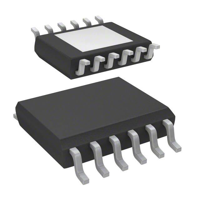


 工商网监
湘ICP备2023018690号
工商网监
湘ICP备2023018690号
