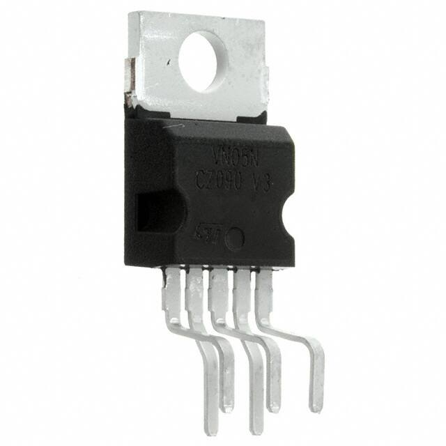
0
登录后你可以
  • 下载海量资料
  • 学习在线课程
  • 观看技术视频
  • 写文章/发帖/加入社区
会员中心
创作中心
发布
  • 发文章

  • 发资料

  • 发帖

  • 提问

  • 发视频

创作活动
VN750-E

VN750-E

  • 厂商:

    STMICROELECTRONICS(意法半导体)

  • 封装:

    Pentawatt5

  • 描述:

    IC PWR DRVR N-CH 1:1 5PENTAWATT

  • 数据手册
  • 价格&库存
VN750-E 数据手册
VN750-E / VN750S-E VN750PT-E / VN750B5-E HIGH SIDE DRIVER Table 1. General Features Type VN750-E VN750B5-E VN750S-E VN750PT RDS(on) 60 mΩ IOUT VCC Figure 1. Package 6A 36 V SO-8 CMOS COMPATIBLE INPUT ON STATE OPEN LOAD DETECTION s OFF STATE OPEN LOAD DETECTION s SHORTED LOAD PROTECTION s UNDERVOLTAGE AND OVERVOLTAGE SHUTDOWN s PROTECTION AGAINST LOSS OF GROUND s VERY LOW STAND-BY CURRENT s s s s PENTAWATT P2PAK PPAK REVERSE BATTERY PROTECTION (*) IN COMPLIANCE WITH THE 2002/95/EC EUROPEAN DIRECTIVE DESCRIPTION The VN750-E, VN750S-E, VN750PT-E, VN750B5-E are a monolithic device designed in STMicroelectronics VIPower M0-3 Technology, intended for driving any kind of load with one side connected to ground. Active VCC pin voltage clamp protects the device against low energy spikes (see ISO7637 transient compatibility table). Active current limitation combined with thermal shutdown and automatic restart protect the device against overload. The device detects open load condition both is on and off state. Output shorted to VCC is detected in the off state. Device automatically turns off in case of ground pin disconnection. Table 2. Order Codes Package PENTAWATT SO-8 P PAK PPAK Note: (*) See application schematic at page 9. 2 Tube VN750-E VN750S-E VN750B5-E VN750PT-E - Tape and Reel VN750STR-E VN750B5TR-E VN750PTTR-E Rev. 1 October 2004 1/31 VN750-E / VN750S-E / VN750PT-E / VN750B5-E Figure 2. Block Diagram VCC VCC CLAMP OVERVOLTAGE DETECTION UNDERVOLTAGE DETECTION GND Power CLAMP INPUT LOGIC DRIVER OUTPUT CURRENT LIMITER STATUS ON STATE OPENLOAD DETECTION OVERTEMPERATURE DETECTION OFF STATE OPENLOAD AND OUTPUT SHORTED TO VCC DETECTION Table 3. Absolute Maximum Ratings Symbol VCC - VCC - Ignd IOUT - IOUT IIN ISTAT Parameter DC Supply Voltage Reverse DC Supply Voltage DC Reverse Ground Pin Current DC Output Current Reverse DC Output Current DC Input Current DC Status Current Electrostatic Discharge (Human Body Model: R=1.5KΩ; C=100pF) VESD - INPUT - STATUS - OUTPUT - VCC Maximum Switching Energy (L=1.8mH; RL=0Ω; Vbat=13.5V; Tjstart=150ºC; IL=9A) Maximum Switching Energy (L=2.46mH; RL=0Ω; Vbat=13.5V; Tjstart=150ºC; IL=9A) Power Dissipation TC=25°C Junction Operating Temperature Case Operating Temperature Storage Temperature 4000 4000 5000 5000 100 138 4.2 60 60 Internally Limited - 40 to 150 - 55 to 150 138 60 V V V V mJ mJ W °C °C °C SO-8 Value PENTAWATT P2PAK 41 - 0.3 - 200 Internally Limited -6 +/- 10 +/- 10 PPAK Unit V V mA A A mA mA EMAX EMAX Ptot Tj Tc Tstg 2/31 VN750-E / VN750S-E / VN750PT-E / VN750B5-E Figure 3. Configuration Diagram (Top View) & Suggested Connections for Unused and N.C. Pins VCC OUTPUT OUTPUT VCC 5 5 4 8 1 N.C. STATUS INPUT GND 4 3 2 1 OUTPUT STATUS VCC INPUT GND SO-8 PPAK / P2PAK PENTAWATT Connection / Pin Status Floating X To Ground N.C. X X Output X Input X Through 10KΩ resistor Figure 4. Current and Voltage Conventions IS VF IIN INPUT ISTAT STATUS GND VIN VSTAT IGND VOUT OUTPUT IOUT VCC VCC Table 4. Thermal Data Symbol Rthj-case Rthj-lead Rthj-amb Parameter Thermal Resistance Junction-case Thermal Resistance Junction-lead Max Max S0-8 30 93 (1) 82 (2) Value PENTAWATT P2PAK 2.1 2.1 62.1 52.1 (3) 62.1 37 (4) PPAK 2.1 77.1 (3) 44 (4) Unit °C/W °C/W °C/W °C/W Thermal Resistance Junction-ambient Max (1) When mounted on a standard single-sided FR-4 board with 0.5cm2 of Cu (at least 35µm thick) connected to all VCC pins. Horizontal mounting and no artificial air flow. (2) When mounted on a standard single-sided FR-4 board with 2cm2 of Cu (at least 35µm thick) connected to all VCC pins. Horizontal mounting and no artificial air flow. (3) When mounted on a standard single-sided FR-4 board with 0.5cm 2 of Cu (at least 35µm thick). Horizontal mounting and no artificial air flow. (4) When mounted on a standard single-sided FR-4 board with 6cm2 of Cu (at least 35µm thick). Horizontal mounting and no artificial air flow. 3/31 VN750-E / VN750S-E / VN750PT-E / VN750B5-E ELECTRICAL CHARACTERISTICS (8VVOV OPEN LOAD without external pull-up INPUT LOAD VOLTAGE STATUS Tj INPUT LOAD CURRENT STATUS TTSD TR OVERTEMPERATURE 8/31 VN750-E / VN750S-E / VN750PT-E / VN750B5-E Figure 8. Application Schematic +5V +5V Rprot STATUS VCC Dld µC Rprot INPUT OUTPUT GND RGND VGND DGND GND PROTECTION REVERSE BATTERY NETWORK AGAINST Solution 1: Resistor in the ground line (RGND only). This can be used with any type of load. The following is an indication on how to dimension the RGND resistor. 1) RGND ≤ 600mV / (IS(on)max). 2) RGND ≥ (−VCC) / (-IGND) where -IGND is the DC reverse ground pin current and can be found in the absolute maximum rating section of the device’s datasheet. Power Dissipation in RGND (when VCC
VN750-E 价格&库存

很抱歉,暂时无法提供与“VN750-E”相匹配的价格&库存,您可以联系我们找货

免费人工找货