物料型号: VN920B5-E
器件简介:
- 该器件是STMicroelectronics™ VIPower™ M0-3技术设计的一款单通道高侧固态继电器(HSD)。
- 它适用于驱动任何类型的负载,其中一侧连接到地。
引脚分配:
- VCC: 电源引脚
- INPUT: 输入引脚
- GND: 地引脚
- OUTPUT: 输出引脚
- C.SENSE: 电流感应引脚
参数特性:
- Rps(on): 16mΩ
- Load current: 30A
- VCC电压: 36V
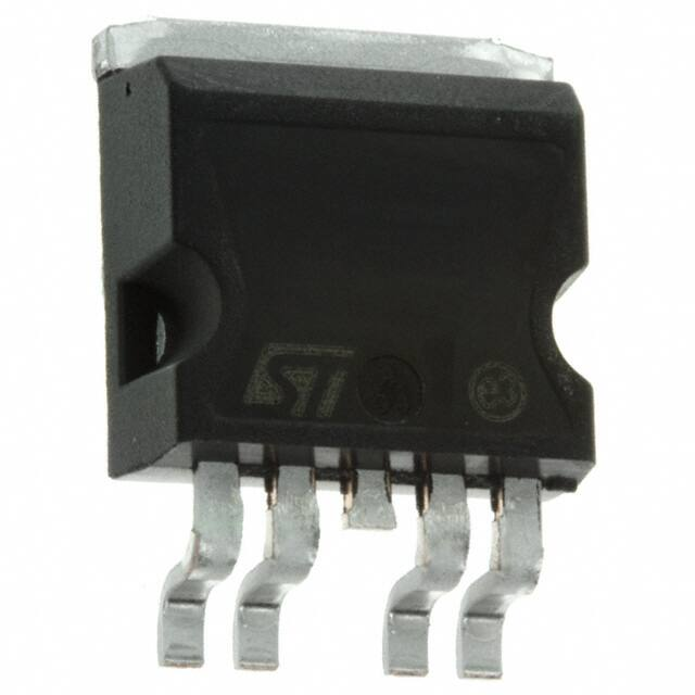
- 封装类型: P2PAK
功能详解:
- 该器件具备多种保护特性,包括热关闭保护、欠压关闭、过压钳位、负载电流限制等。
- 集成了模拟电流感应输出,提供与负载电流成比例的电流。
- 设备在地引脚断开时自动关闭。
应用信息:
- 提供了关于GND保护网络、负载转储保护、MCU I/Os保护等应用信息。
- 包括了针对不同情况的解决方案和计算公式。
封装信息:
- 提供了P2PAK封装的详细信息,包括热数据、机械数据和包装信息。