VN920SP
Single channel high-side solid-state relay
Features
Type
VN920SP
RDS(on)
IOUT
VCC
15 mΩ
30 A
36 V
10
)
s
(
t
PowerSO-10 c
u
d
o
r
Description P
e
t
e
l
o
s
b
-O
1
■
CMOS compatible input
■
Proportional load current sense
■
Shorted load protection
■
Under-voltage and over-voltage shutdown
■
Over-voltage clamp
■
Thermal shutdown
■
Current limitation
■
Protection against loss of ground and loss of
VCC
■
Very low standby power dissipation
■
Reverse battery protected (see Application
schematic )
)
s
(
ct
u
d
o
r
P
e
t
e
l
o
s
b
O
Table 1.
The VN920SP is a monolithic device designed in
STMicroelectronics VIPower M0-3 technology.
The VN920SP is intended for driving any type of
load with one side connected to ground. The
active VCC pin voltage clamp protects the device
against low energy spikes (see ISO7637 transient
compatibility table). Active current limitation
combined with thermal shutdown and automatic
restart protects the device against over-load.
The device integrates an analog current sense
output which delivers a current proportional to the
load current. The device automatically turns off in
the case where the ground pin becomes
disconnected.
Device summary
Order codes
Package
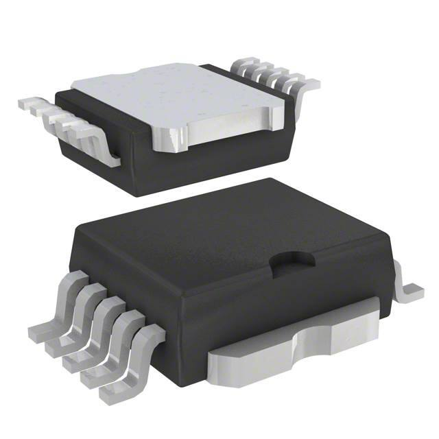
PowerSO-10
September 2013
Tube
Tape and reel
VN920SP
VN920SP13TR
DocID7372 Rev 4
1/26
www.st.com
26
�Contents
VN920SP
Contents
1
Block diagram and pin description . . . . . . . . . . . . . . . . . . . . . . . . . . . . . 5
2
Electrical specifications . . . . . . . . . . . . . . . . . . . . . . . . . . . . . . . . . . . . . . 6
3
2.1
Absolute maximum ratings . . . . . . . . . . . . . . . . . . . . . . . . . . . . . . . . . . . . . 6
2.2
Thermal data . . . . . . . . . . . . . . . . . . . . . . . . . . . . . . . . . . . . . . . . . . . . . . . 7
2.3
Electrical characteristics . . . . . . . . . . . . . . . . . . . . . . . . . . . . . . . . . . . . . . . 8
2.4
Electrical characteristics curves . . . . . . . . . . . . . . . . . . . . . . . . . . . . . . . . 14
)
s
(
ct
u
d
o
Application information . . . . . . . . . . . . . . . . . . . . . . . . . . . . . . . . . . . . . 16
3.1
4
GND protection network against reverse battery . . . . . . . . . . . . . . . . . . . 16
r
P
e
3.1.1
Solution 1: resistor in the ground line (RGND only) . . . . . . . . . . . . . . . . 16
3.1.2
Solution 2: diode (DGND) in the ground line . . . . . . . . . . . . . . . . . . . . . 17
t
e
l
o
3.2
Load dump protection . . . . . . . . . . . . . . . . . . . . . . . . . . . . . . . . . . . . . . . . 17
3.3
MCU I/Os protection . . . . . . . . . . . . . . . . . . . . . . . . . . . . . . . . . . . . . . . . . 17
3.4
PowerSO-10 maximum demagnetization energy (VCC = 13.5V) . . . . . . . 18
)
(s
s
b
O
Package and PCB thermal data . . . . . . . . . . . . . . . . . . . . . . . . . . . . . . . 19
4.1
5
t
c
u
PowerSO-10 thermal data . . . . . . . . . . . . . . . . . . . . . . . . . . . . . . . . . . . . 19
d
o
r
Package and packing information . . . . . . . . . . . . . . . . . . . . . . . . . . . . . 22
P
e
5.1
t
e
l
o
s
b
O
6
2/26
ECOPACK® packages . . . . . . . . . . . . . . . . . . . . . . . . . . . . . . . . . . . . . . . 22
5.2
PowerSO-10 mechanical data . . . . . . . . . . . . . . . . . . . . . . . . . . . . . . . . . 22
5.3
PowerSO-10 packing information . . . . . . . . . . . . . . . . . . . . . . . . . . . . . . . 24
Revision history . . . . . . . . . . . . . . . . . . . . . . . . . . . . . . . . . . . . . . . . . . . 25
�VN920SP
List of tables
List of tables
Table 1.
Table 2.
Table 3.
Table 4.
Table 5.
Table 6.
Table 7.
Table 8.
Table 9.
Table 10.
Table 11.
Table 12.
Table 13.
Table 14.
Table 15.
Device summary . . . . . . . . . . . . . . . . . . . . . . . . . . . . . . . . . . . . . . . . . . . . . . . . . . . . . . . . . . 1
Suggested connections for unused and not connected pins . . . . . . . . . . . . . . . . . . . . . . . . 5
Absolute maximum ratings . . . . . . . . . . . . . . . . . . . . . . . . . . . . . . . . . . . . . . . . . . . . . . . . . . 6
Thermal data. . . . . . . . . . . . . . . . . . . . . . . . . . . . . . . . . . . . . . . . . . . . . . . . . . . . . . . . . . . . . 7
Power . . . . . . . . . . . . . . . . . . . . . . . . . . . . . . . . . . . . . . . . . . . . . . . . . . . . . . . . . . . . . . . . . . 8
Switching (VCC=13V) . . . . . . . . . . . . . . . . . . . . . . . . . . . . . . . . . . . . . . . . . . . . . . . . . . . . . . 8
Logic inputs. . . . . . . . . . . . . . . . . . . . . . . . . . . . . . . . . . . . . . . . . . . . . . . . . . . . . . . . . . . . . . 9
Current sense (9V ≤VCC ≤16V) . . . . . . . . . . . . . . . . . . . . . . . . . . . . . . . . . . . . . . . . . . . . . . 9
VCC output diode. . . . . . . . . . . . . . . . . . . . . . . . . . . . . . . . . . . . . . . . . . . . . . . . . . . . . . . . . 10
Protections . . . . . . . . . . . . . . . . . . . . . . . . . . . . . . . . . . . . . . . . . . . . . . . . . . . . . . . . . . . . . 10
Truth table. . . . . . . . . . . . . . . . . . . . . . . . . . . . . . . . . . . . . . . . . . . . . . . . . . . . . . . . . . . . . . 11
Electrical transient requirements . . . . . . . . . . . . . . . . . . . . . . . . . . . . . . . . . . . . . . . . . . . . 11
Thermal parameters . . . . . . . . . . . . . . . . . . . . . . . . . . . . . . . . . . . . . . . . . . . . . . . . . . . . . . 21
PowerSO-10 mechanical data . . . . . . . . . . . . . . . . . . . . . . . . . . . . . . . . . . . . . . . . . . . . . . 23
Document revision history . . . . . . . . . . . . . . . . . . . . . . . . . . . . . . . . . . . . . . . . . . . . . . . . . 25
)
s
(
ct
u
d
o
r
P
e
t
e
l
o
)
(s
s
b
O
t
c
u
d
o
r
P
e
t
e
l
o
s
b
O
3/26
�List of figures
VN920SP
List of figures
Figure 1.
Figure 2.
Figure 3.
Figure 4.
Figure 5.
Figure 6.
Figure 7.
Figure 8.
Figure 9.
Figure 10.
Figure 11.
Figure 12.
Figure 13.
Figure 14.
Figure 15.
Figure 16.
Figure 17.
Figure 18.
Figure 19.
Figure 20.
Figure 21.
Figure 22.
Figure 23.
Figure 24.
Figure 25.
Figure 26.
Figure 27.
Figure 28.
Block diagram . . . . . . . . . . . . . . . . . . . . . . . . . . . . . . . . . . . . . . . . . . . . . . . . . . . . . . . . . . . . 5
Configuration diagram (top view) . . . . . . . . . . . . . . . . . . . . . . . . . . . . . . . . . . . . . . . . . . . . . 5
Current and voltage conventions . . . . . . . . . . . . . . . . . . . . . . . . . . . . . . . . . . . . . . . . . . . . . 6
Switching characteristics . . . . . . . . . . . . . . . . . . . . . . . . . . . . . . . . . . . . . . . . . . . . . . . . . . 12
IOUT/ISENSE versus IOUT . . . . . . . . . . . . . . . . . . . . . . . . . . . . . . . . . . . . . . . . . . . . . . . . . . . 12
Waveforms . . . . . . . . . . . . . . . . . . . . . . . . . . . . . . . . . . . . . . . . . . . . . . . . . . . . . . . . . . . . . 13
Off-state output current . . . . . . . . . . . . . . . . . . . . . . . . . . . . . . . . . . . . . . . . . . . . . . . . . . . . 14
High-level input current . . . . . . . . . . . . . . . . . . . . . . . . . . . . . . . . . . . . . . . . . . . . . . . . . . . . 14
Input clamp voltage. . . . . . . . . . . . . . . . . . . . . . . . . . . . . . . . . . . . . . . . . . . . . . . . . . . . . . . 14
Turn-on voltage slope . . . . . . . . . . . . . . . . . . . . . . . . . . . . . . . . . . . . . . . . . . . . . . . . . . . . . 14
Over-voltage shutdown . . . . . . . . . . . . . . . . . . . . . . . . . . . . . . . . . . . . . . . . . . . . . . . . . . . . 14
Turn-off voltage slope . . . . . . . . . . . . . . . . . . . . . . . . . . . . . . . . . . . . . . . . . . . . . . . . . . . . . 14
ILIM vs Tcase . . . . . . . . . . . . . . . . . . . . . . . . . . . . . . . . . . . . . . . . . . . . . . . . . . . . . . . . . . . 15
On-state resistance vs VCC . . . . . . . . . . . . . . . . . . . . . . . . . . . . . . . . . . . . . . . . . . . . . . . . 15
Input high-level . . . . . . . . . . . . . . . . . . . . . . . . . . . . . . . . . . . . . . . . . . . . . . . . . . . . . . . . . . 15
Input hysteresis voltage . . . . . . . . . . . . . . . . . . . . . . . . . . . . . . . . . . . . . . . . . . . . . . . . . . . 15
On-state resistance vs Tcase . . . . . . . . . . . . . . . . . . . . . . . . . . . . . . . . . . . . . . . . . . . . . . . 15
Input low-level . . . . . . . . . . . . . . . . . . . . . . . . . . . . . . . . . . . . . . . . . . . . . . . . . . . . . . . . . . . 15
Application schematic . . . . . . . . . . . . . . . . . . . . . . . . . . . . . . . . . . . . . . . . . . . . . . . . . . . . . 16
PowerSO-10 maximum turn-off current versus inductance . . . . . . . . . . . . . . . . . . . . . . . . 18
PowerSO-10 PC board . . . . . . . . . . . . . . . . . . . . . . . . . . . . . . . . . . . . . . . . . . . . . . . . . . . . 19
Rthj-amb Vs PCB copper area in open box free air condition . . . . . . . . . . . . . . . . . . . . . . 19
Thermal impedance junction ambient single pulse . . . . . . . . . . . . . . . . . . . . . . . . . . . . . . 20
Thermal fitting model of a single channel HSD in PowerSO-10 . . . . . . . . . . . . . . . . . . . . . 20
PowerSO-10 package dimensions . . . . . . . . . . . . . . . . . . . . . . . . . . . . . . . . . . . . . . . . . . . 22
PowerSO-10 suggested pad layout . . . . . . . . . . . . . . . . . . . . . . . . . . . . . . . . . . . . . . . . . . 24
PowerSO-10 tube shipment (no suffix) . . . . . . . . . . . . . . . . . . . . . . . . . . . . . . . . . . . . . . . . 24
PowerSO-10 tape and reel shipment (suffix “TR”) . . . . . . . . . . . . . . . . . . . . . . . . . . . . . . . 24
)
s
(
ct
u
d
o
r
P
e
t
e
l
o
)
(s
t
c
u
P
e
d
o
r
t
e
l
o
s
b
O
4/26
s
b
O
�VN920SP
1
Block diagram and pin description
Block diagram and pin description
Figure 1.
Block diagram
VCC
OVERVOLTAGE
DETECTION
VCC
CLAMP
UNDERVOLTAGE
DETECTION
GND
)
s
(
ct
Power CLAMP
u
d
o
DRIVER
LOGIC
INPUT
r
P
e
CURRENT LIMITER
VDS LIMITER
let
IOUT
o
s
b
OVERTEMPERATURE
DETECTION
Figure 2.
CURRENT
SENSE
K
O
)
s
(
t
c
Configuration diagram (top view)
u
d
o
e
t
e
l
OUTPUT
Pr
o
s
b
GROUND
INPUT
C.SENSE
N.C.
N.C.
6
5
OUTPUT
7
4
8
3
OUTPUT
N.C.
9
2
OUTPUT
10
1
OUTPUT
11
VCC
O
PowerSO-10
Table 2.
Suggested connections for unused and not connected pins
Connection / pin
Current Sense
Floating
To ground
Through 1KΩ
resistor
N.C.
Output
Input
X
X
X
X
Through 10KΩ
resistor
5/26
�Electrical specifications
2
VN920SP
Electrical specifications
Figure 3.
Current and voltage conventions
IS
VCC
VF
VCC
IOUT
OUTPUT
IIN
VOUT
INPUT
VIN
)
s
(
ct
ISENSE
CURRENT SENSE
VSENSE
u
d
o
GND
r
P
e
IGND
2.1
t
e
l
o
s
b
O
Absolute maximum ratings
Stressing the device above the rating listed in the “Absolute maximum ratings” table may
cause permanent damage to the device. These are stress ratings only and operation of the
device at these or any other conditions above those indicated in the operating sections of
this specification is not implied. Exposure to Absolute maximum rating conditions for
extended periods may affect device reliability. Refer also to the STMicroelectronics sure
program and other relevant quality document.
)
(s
t
c
u
Table 3.
P
e
VCC
DC supply voltage
- VCC
Symbol
Value
Unit
41
V
Reverse DC supply voltage
- 0.3
V
- Ignd
DC reverse ground pin current
- 200
mA
IOUT
DC output current
Internally limited
A
- IOUT
Reverse DC output current
- 40
A
DC input current
+/- 10
mA
Current Sense maximum voltage
-3
+ 15
V
V
4000
2000
5000
5000
V
V
V
V
t
e
l
o
s
b
O
IIN
VCSENSE
VESD
6/26
d
o
r
Absolute maximum ratings
Parameter
Electrostatic discharge
(human body model: R = 1.5KΩ; C = 100pF)
INPUT
CURRENT SENSE
OUTPUT
VCC
�VN920SP
Electrical specifications
Table 3.
Absolute maximum ratings (continued)
Symbol
Parameter
EMAX
Ptot
Unit
Maximum switching energy
(L = 0.25mH; RL= 0Ω; Vbat = 13.5V;
Tjstart = 150ºC; IL = 45A)
362
mJ
Power dissipation TC ≤25°C
96.1
W
Internally limited
°C
Tj
Junction operating temperature
Tc
Case operating temperature
- 40 to 150
°C
Storage temperature
- 55 to 150
°C
Tstg
2.2
Value
)
s
(
ct
Thermal data
Table 4.
u
d
o
Thermal data
Symbol
Parameter
Rthj-case
Thermal resistance junction-case
Rthj-amb
Thermalresistance junction-ambient
s
b
O
e
t
e
ol
Pr
Max. value
Unit
1.3
°C/W
51.3(1)
1.
When mounted on FR4 printed circuit board with 0.5cm2 of Cu (at least 35µm thick).
2.
When mounted on FR4 printed circuit board with 6cm2 of Cu (at least 35µm thick).
)
(s
37(2)
°C/W
°C/W
t
c
u
d
o
r
P
e
t
e
l
o
s
b
O
7/26
�Electrical specifications
2.3
VN920SP
Electrical characteristics
Values specified in this section are for 8V < VCC < 36V; -40°C < Tj < 150°C, unless otherwise
stated.
Table 5.
Power
Symbol
Parameter
VCC
Test conditions
Min.
Typ.
Operating supply voltage
5.5
13
36
V
VUSD
Under-voltage shutdown
3
4
5.5
V
VOV
Over-voltage shutdown
36
RON
On-state resistance
ICC = 20mA
Off-state; VCC = 13V;
VIN = VOUT = 0V
e
t
e
ol
Off-state; VCC = 13V;
VIN = VOUT = 0V; Tj = 25°C
Supply current
IS
V
IOUT = 10A; Tj = 25°C;
IOUT = 10A;
IOUT = 3A; VCC = 6V
VCLAMP Clamp voltage
Off-state output current
IL(off2)
Off-state output current
IL(off3)
Off-state output current
IL(off4)
e
t
e
ol
Note:
bs
O
8/26
du
o
r
P
Off-state output current
mΩ
mΩ
mΩ
du
41
48
55
V
o
r
P
10
25
µA
10
20
µA
5
mA
s
b
O
0
50
µA
VIN = 0V; VOUT = 3.5V
-75
0
µA
VIN = VOUT = 0V; VCC = 13V;
Tj = 125°C
5
µA
VIN = VOUT = 0V; VCC = 13V;
Tj = 25°C
3
µA
)-
s
(
t
c
15
30
50
)
s
(
ct
On-state; VCC = 13V; VIN = 5V;
IOUT = 0A; RSENSE = 3.9 kΩ
IL(off1)
Max. Unit
VIN = VOUT = 0V
VCLAMP and VOV are correlated. Typical difference is 5V.
Table 6.
Symbol
Switching (VCC=13V)
Parameter
Test conditions
Min.
Typ.
Max. Unit
td(on)
Turn-on delay time
RL = 1.3Ω (see Figure 4.)
50
µs
td(off)
Turn-off delay time
RL = 1.3Ω (see Figure 4.)
50
µs
dVOUT/dt(on) Turn-on voltage slope RL = 1.3Ω (see Figure 4.)
See Figure 10.
V/µs
dVOUT/dt(off) Turn-off voltage slope RL = 1.3Ω (see Figure 4.)
See Figure 12.
V/µs
�VN920SP
Electrical specifications
Table 7.
Logic inputs
Symbol
Parameter
VIL
Input low-level voltage
IIL
Low-level input current
VIH
Input high-level voltage
IIH
High-level input current
VI(hyst)
Input hysteresis voltage
VICL
K1
dK1/K1
K2
dK2/K2
K3
b
O
ISENSE0
VSENSE
VSENSEH
Typ.
Unit
1.25
V
µA
3.25
V
10
0.5
IIN = 1mA
IIN = - 1mA
Test conditions
IOUT/ISENSE
IOUT = 1A; VSENSE = 0.5V;
Tj = -40°C...150°C
Current sense
ratio drift
IOUT = 1A; VSENSE = 0.5V;
Tj= - 40°C...150°C
IOUT/ISENSE
IOUT = 10A; VSENSE = 4V;
Tj = - 40°C
Tj= 25°C...150°C
Current sense
ratio drift
IOUT = 10A; VSENSE = 4V;
Tj = -40°C...150°C
IOUT/ISENSE
IOUT = 30A; VSENSE = 4V;
Tj = -40°C
Tj = 25°C...150°C
e
t
e
l
o
s
b
O
)
s
(
t
c
u
d
o
Max.
1
VIN = 3.25V
Parameter
Pr
dK3/K3
Min.
6
6.8
- 0.7
8
Current sense
ratio drift
IOUT = 30A; VSENSE = 4V;
Tj = -40°C...150°C
Analog sense
current
VCC = 6...16V; IOUT = 0A;
VSENSE = 0V;
Tj = -40°C...150°C
Max analog
sense output
voltage
VCC = 5.5V; IOUT = 5A;
RSENSE = 10kΩ
VCC > 8V, IOUT = 10A;
RSENSE = 10kΩ
Sense voltage in
over-temperature VCC = 13V; RSENSE = 3.9kΩ
condition
o
r
P
Typ.
4400
-10
4200
4400
-8
4200
4400
Max.
%
6000
5750
+8
4900
4900
Unit
6000
+10
4900
4900
V
V
)
s
(
ct
du
Min.
3300
µA
V
Current sense (9V ≤VCC ≤16V)
Symbol
e
t
e
l
VIN = 1.25V
Input clamp voltage
Table 8.
so
Test conditions
%
5500
5250
-6
+6
%
0
10
µA
2
V
4
V
5.5
V
9/26
�Electrical specifications
Table 8.
Symbol
VN920SP
Current sense (9V ≤VCC ≤16V) (continued)
Parameter
Test conditions
Min.
Typ.
Analog sense
output
VCC = 13V; Tj > TTSD;
RVSENSEH impedance in
output open
over-temperature
condition
tDSENSE
Current sense
delay response
Max.
Unit
Ω
400
To 90% ISENSE(1)
500
µs
1. Current sense signal delay after positive input slope.
Table 9.
Symbol
Parameter
Test conditions
VF
Forward on voltage
- IOUT = 5.3A; Tj = 150°C
Table 10.
Protections(1)
Symbol
Parameter
TTSD
TR
Reset temperature
Thyst
Thermal hysteresis
Current limitation
Vdemag
VON
e
t
e
ol
s
b
O
10/26
o
r
P
du
Output voltage drop
limitation
o
s
b
O
)
s
(
t
c
Turn-off output clamp
voltage
Min.
VCC = 13V
5V < VCC < 36V
Typ.
u
d
o
r
P
e
let
Test conditions
Shutdown temperature
Ilim
)
s
(
ct
VCC output diode
Max.
Unit
0.6
V
Min.
Typ.
Max.
Unit
150
175
200
°C
135
°C
7
15
30
45
°C
75
75
A
A
IOUT = 2 A;
VIN = 0V;
L = 6mH
VCC - 41 VCC - 48 VCC - 55
V
IOUT = 1 A;
Tj = -40°C...150°C
50
mV
1. To ensure long term reliability under heavy over-load or short circuit conditions, protection and related
diagnostic signals must be used together with a proper software strategy. If the device operates under
abnormal conditions this software must limit the duration and number of activation cycles.
�VN920SP
Electrical specifications
Table 11.
Truth table
Conditions
Input
Output
Sense
Normal operation
L
H
L
H
0
Nominal
Over-temperature
L
H
L
L
0
VSENSEH
Under-voltage
L
H
L
L
0
0
Over-voltage
L
H
L
L
0
0
Short circuit to GND
L
H
H
L
L
L
Short circuit to VCC
L
H
H
H
Negative output voltage clamp
L
Table 12.
Test pulse
I
1
- 25V(1)
2
+ 25V(1)
Pr
e
t
e
l
o
s
b
5
(1)
- 25V
+ 25V
-
)II
s
b
O
0
(1)
4V(1)
+ 26.5V(1)
III
IV
Delays and impedance
- 50V(1)
- 75V(1)
- 100V(1)
2ms, 10Ω
+ 50V(1)
+ 75V(1)
+ 100V(1)
0.2ms, 10Ω
-
50V(1)
100V(1)
-
150V(1)
0.1µs, 50Ω
+
50V(1)
+
100V(1)
0.1µs, 50Ω
-
5V(1)
7V(1)
100ms, 0.01Ω
t(s
uc
od
3a
4
t
e
l
o
L
0
< Nominal
Test level
7637/1
3b
u
d
o
r
P
e
Electrical transient requirements
ISO T/R
)
s
(
ct
0
(TjTTSD) VSENSEH
+ 46.5V(2)
-
+
75V(1)
-
6V(1)
+ 66.5V(2)
-
+ 86.5V(2)
400ms, 2Ω
1. All functions of the device are performed as designed after exposure to disturbance.
2. One or more functions of the device is not performed as designed after exposure and cannot be returned to
proper operation without replacing the device.
O
11/26
�Electrical specifications
Figure 4.
VN920SP
Switching characteristics
VOUT
90%
80%
dVOUT/dt(off)
dVOUT/dt(on)
10%
tr
tf
t
ISENSE
90%
t
u
d
o
tDSENSE
INPUT
td(on)
)
s
(
ct
td(off)
r
P
e
t
e
l
o
Figure 5.
)
(s
IOUT/ISENSE versus IOUT
IOUT/ISENSE
d
o
r
P
e
5500
t
e
l
o
s
b
O
s
b
O
t
c
u
6500
6000
t
max.Tj=-40°C
max.Tj=25...150°C
5000
typical value
min.Tj=25...150°C
4500
min.Tj=-40°C
4000
3500
3000
0
2
4
6
8
10
12
14
16
IOUT (A)
12/26
18
20
22
24
26
28
30
32
�VN920SP
Electrical specifications
Figure 6.
Waveforms
NORMAL OPERATION
INPUT
LOAD CURRENT
SENSE
UNDERVOLTAGE
VCC
VUSDhyst
VUSD
INPUT
)
s
(
ct
LOAD CURRENT
SENSE
u
d
o
OVERVOLTAGE
r
P
e
VOV
VCC
VOVhyst
VCC > VUSD
INPUT
LOAD CURRENT
SENSE
t
e
l
o
s
b
O
SHORT TO GROUND
INPUT
)
(s
LOAD CURRENT
LOAD VOLTAGE
SENSE
od
r
P
e
INPUT
s
b
O
t
e
l
o
t
c
u
SHORT TO VCC
LOAD VOLTAGE
LOAD CURRENT
SENSE
很抱歉,暂时无法提供与“VN920SP13TR”相匹配的价格&库存,您可以联系我们找货
免费人工找货- 国内价格 香港价格
- 600+20.07597600+2.59737