物料型号:VND10B
器件简介:VND10B是使用STMicroelectronics VIPower技术制造的单片设备,用于驱动具有一侧接地的电阻性或感性负载。该设备有两个通道和一个公共诊断。内置的热关闭功能可保护芯片免受过温和短路的影响。
引脚分配:文档中提供了连接图,展示了输入、输出、Vcc、GND和诊断引脚的分配。
参数特性:
- 工作电压(Vcc):6V至26V
- 通态电阻(RDS(on)):最大0.1欧姆
- 额定电流(In):3.4A(在85°C时,电池电压13V产生0.5V的电压降)
- 连续输出电流:每通道14A(在85°C时)
- 热关闭:在过温和短路时保护芯片
- 诊断输出:提供开路负载、过温和粘连到VCC状态的指示
功能详解:
- 热关闭:在结温达到140°C时关闭功率MOSFET,当温度降至125°C时自动重新打开。
- 快速退磁:内部功能确保感性负载的快速退磁,典型退磁电压为-18V。
- 诊断输出:提供两个通道的共同诊断输出,指示开路负载、过温和粘连到VCC状态。
应用信息:适用于汽车开关应用,具有5V逻辑电平兼容的输入。
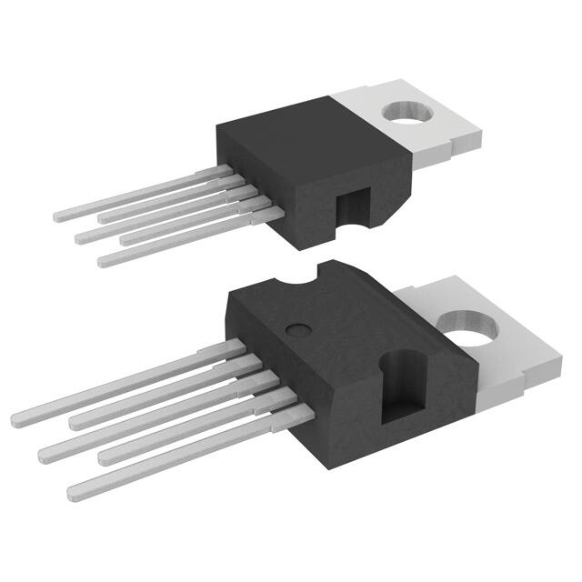
封装信息:提供PENTAWATT垂直、水平和内联三种封装方式的详细机械数据和尺寸图。