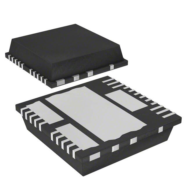
VND5004B-E
VND5004BSP30-E
Double 4 mhigh-side driver with analog current sense
for automotive applications
Datasheet - production data
–
–
–
–
–
–
Undervoltage shutdown
Overvoltage clamp
Load current limitation
Thermal shutdown
Self limiting of fast thermal transients
Protection against loss of ground and loss
of VCC
– Reverse battery protection with self switch
on of the Power MOSFET
– Electrostatic discharge protection
application
All types of resistive, inductive and capacitive
loads
PQFN
12x12 Power lead-less
MultiPowerSO-30
Features
Parameters
Symbol
Value
Max transient supply voltage
VCC
41 V
Operating voltage range
VCC
4.5 to 28 V
Description
Max on-state resistance
RON
4 m
Current limitation (typ)
ILIMH
100 A
Off-state supply current
IS
2 µA(1)
1. Typical value with all loads connected.
AEC-Q100 qualified
General
– Inrush current active management by
power limitation
– Very low standby current
– 3.0 V CMOS compatible input
– Optimized electromagnetic emission
– Very low electromagnetic susceptibility
– In compliance with the 2002/95/EC
European directive
Diagnostic functions
– Proportional load current sense
– Current sense disable
– Thermal shutdown indication
Protection
Suitable for power management applications
The VND5004B-E and VND5004BSP30-E are
devices made using STMicroelectronics VIPower
technology. They are intended for driving resistive
or inductive loads with one side connected to
ground. Active VCC pin voltage clamp and load
dump protection circuit protect the devices
against transients on the Vcc pin. These devices
integrate an analog current sense which delivers
a current proportional to the load current
(according to a known ratio) when CS_DIS is
driven low or left open. When CS_DIS is driven
high, the CURRENT SENSE pin is high
impedance. Output current limitation protects the
devices in overload condition. In case of long
duration overload, the devices limit the dissipated
power to a safe level up to thermal shutdown
intervention. Thermal shutdown with automatic
restart allows the device to recover normal
operation as soon as a fault condition disappears.
Table 1. Device summary
Package
PQFN-12x12 power lead-less
MultiPowerSO-30
January 2017
This is information on a product in full production.
Order codes
Tape and reel
VND5004BTR-E
VND5004BSP30TR-E
DocID15702 Rev 4
Tray
VND5004B-E
-
1/33
www.st.com
�Contents
VND5004B-E, VND5004BSP30-E
Contents
1
Block diagram and pin configurations . . . . . . . . . . . . . . . . . . . . . . . . . . 5
2
Electrical specifications . . . . . . . . . . . . . . . . . . . . . . . . . . . . . . . . . . . . . . 7
3
4
5
6
2/33
2.1
Absolute maximum ratings . . . . . . . . . . . . . . . . . . . . . . . . . . . . . . . . . . . . . 7
2.2
Thermal data . . . . . . . . . . . . . . . . . . . . . . . . . . . . . . . . . . . . . . . . . . . . . . . 8
2.3
Electrical characteristics . . . . . . . . . . . . . . . . . . . . . . . . . . . . . . . . . . . . . . . 9
2.4
Electrical characteristics curves . . . . . . . . . . . . . . . . . . . . . . . . . . . . . . . . 15
Application information . . . . . . . . . . . . . . . . . . . . . . . . . . . . . . . . . . . . . 18
3.1
Microcontroller I/Os protection . . . . . . . . . . . . . . . . . . . . . . . . . . . . . . . . . 18
3.2
Load dump protection . . . . . . . . . . . . . . . . . . . . . . . . . . . . . . . . . . . . . . . . 18
3.3
Maximum demagnetization energy (VCC = 13.5 V) . . . . . . . . . . . . . . . . . 19
Package and PC board thermal data . . . . . . . . . . . . . . . . . . . . . . . . . . . 20
4.1
MultiPowerSO-30 thermal data . . . . . . . . . . . . . . . . . . . . . . . . . . . . . . . . 20
4.2
PQFN - 12x12 power lead-less thermal data . . . . . . . . . . . . . . . . . . . . . . 22
Package information . . . . . . . . . . . . . . . . . . . . . . . . . . . . . . . . . . . . . . . . 25
5.1
MultiPowerSO-30 package information . . . . . . . . . . . . . . . . . . . . . . . . . . 25
5.2
PQFN - 12x12 power lead-less package information . . . . . . . . . . . . . . . . 27
5.3
MultiPowerSO-30 packing information . . . . . . . . . . . . . . . . . . . . . . . . . . . 29
5.4
PQFN - 12x12 power lead-less packing information . . . . . . . . . . . . . . . . 30
Revision history . . . . . . . . . . . . . . . . . . . . . . . . . . . . . . . . . . . . . . . . . . . 32
DocID15702 Rev 4
�VND5004B-E, VND5004BSP30-E
List of tables
List of tables
Table 1.
Table 2.
Table 3.
Table 4.
Table 5.
Table 6.
Table 7.
Table 8.
Table 9.
Table 10.
Table 11.
Table 12.
Table 13.
Table 14.
Table 15.
Device summary . . . . . . . . . . . . . . . . . . . . . . . . . . . . . . . . . . . . . . . . . . . . . . . . . . . . . . . . . . 1
Pin functions . . . . . . . . . . . . . . . . . . . . . . . . . . . . . . . . . . . . . . . . . . . . . . . . . . . . . . . . . . . . . 5
Suggested connections for unused and not connected pins . . . . . . . . . . . . . . . . . . . . . . . . 6
Absolute maximum ratings . . . . . . . . . . . . . . . . . . . . . . . . . . . . . . . . . . . . . . . . . . . . . . . . . . 7
Thermal data. . . . . . . . . . . . . . . . . . . . . . . . . . . . . . . . . . . . . . . . . . . . . . . . . . . . . . . . . . . . . 8
Electrical characteristics . . . . . . . . . . . . . . . . . . . . . . . . . . . . . . . . . . . . . . . . . . . . . . . . . . . . 9
Truth table. . . . . . . . . . . . . . . . . . . . . . . . . . . . . . . . . . . . . . . . . . . . . . . . . . . . . . . . . . . . . . 12
Electrical transient requirements (part 1/3) . . . . . . . . . . . . . . . . . . . . . . . . . . . . . . . . . . . . . 13
Electrical transient requirements (part 2/3) . . . . . . . . . . . . . . . . . . . . . . . . . . . . . . . . . . . . . 13
Electrical transient requirements (part 3/3) . . . . . . . . . . . . . . . . . . . . . . . . . . . . . . . . . . . . . 13
Thermal parameters for MultiPowerSO-30 . . . . . . . . . . . . . . . . . . . . . . . . . . . . . . . . . . . . . 22
Thermal parameters for PQFN - 12x12 power lead-less . . . . . . . . . . . . . . . . . . . . . . . . . . 24
MultiPowerSO-30 mechanical data . . . . . . . . . . . . . . . . . . . . . . . . . . . . . . . . . . . . . . . . . . 25
PQFN - 12x12 power lead-less mechanical data . . . . . . . . . . . . . . . . . . . . . . . . . . . . . . . . 28
Document revision history . . . . . . . . . . . . . . . . . . . . . . . . . . . . . . . . . . . . . . . . . . . . . . . . . 32
DocID15702 Rev 4
3/33
3
�List of figures
VND5004B-E, VND5004BSP30-E
List of figures
Figure 1.
Block diagram . . . . . . . . . . . . . . . . . . . . . . . . . . . . . . . . . . . . . . . . . . . . . . . . . . . . . . . . . . . . 5
Figure 2.
Configuration diagram (not to scale) . . . . . . . . . . . . . . . . . . . . . . . . . . . . . . . . . . . . . . . . . . 6
Figure 3.
Current and voltage conventions . . . . . . . . . . . . . . . . . . . . . . . . . . . . . . . . . . . . . . . . . . . . . 7
Figure 4.
Current sense delay characteristics . . . . . . . . . . . . . . . . . . . . . . . . . . . . . . . . . . . . . . . . . . 11
Figure 5.
Switching characteristics . . . . . . . . . . . . . . . . . . . . . . . . . . . . . . . . . . . . . . . . . . . . . . . . . . 12
Figure 6.
Waveforms . . . . . . . . . . . . . . . . . . . . . . . . . . . . . . . . . . . . . . . . . . . . . . . . . . . . . . . . . . . . . 14
Figure 7.
Off-state output current . . . . . . . . . . . . . . . . . . . . . . . . . . . . . . . . . . . . . . . . . . . . . . . . . . . . 15
Figure 8.
High level input current . . . . . . . . . . . . . . . . . . . . . . . . . . . . . . . . . . . . . . . . . . . . . . . . . . . . 15
Figure 9.
Input clamp voltage. . . . . . . . . . . . . . . . . . . . . . . . . . . . . . . . . . . . . . . . . . . . . . . . . . . . . . . 15
Figure 10. Input low level . . . . . . . . . . . . . . . . . . . . . . . . . . . . . . . . . . . . . . . . . . . . . . . . . . . . . . . . . . . 15
Figure 11. Input high level . . . . . . . . . . . . . . . . . . . . . . . . . . . . . . . . . . . . . . . . . . . . . . . . . . . . . . . . . . 15
Figure 12. Input hysteresis voltage . . . . . . . . . . . . . . . . . . . . . . . . . . . . . . . . . . . . . . . . . . . . . . . . . . . 15
Figure 13. On-state resistance vs Tcase . . . . . . . . . . . . . . . . . . . . . . . . . . . . . . . . . . . . . . . . . . . . . . . . 16
Figure 14. On-state resistance vs VCC. . . . . . . . . . . . . . . . . . . . . . . . . . . . . . . . . . . . . . . . . . . . . . . . . 16
Figure 15. Undervoltage shutdown . . . . . . . . . . . . . . . . . . . . . . . . . . . . . . . . . . . . . . . . . . . . . . . . . . . 16
Figure 16. Turn-on voltage slope . . . . . . . . . . . . . . . . . . . . . . . . . . . . . . . . . . . . . . . . . . . . . . . . . . . . . 16
Figure 17. ILIMH vs Tcase . . . . . . . . . . . . . . . . . . . . . . . . . . . . . . . . . . . . . . . . . . . . . . . . . . . . . . . . . . . 16
Figure 18. Turn-off voltage slope . . . . . . . . . . . . . . . . . . . . . . . . . . . . . . . . . . . . . . . . . . . . . . . . . . . . . 16
Figure 19. CS_DIS high level voltage . . . . . . . . . . . . . . . . . . . . . . . . . . . . . . . . . . . . . . . . . . . . . . . . . 17
Figure 20. CS_DIS clamp voltage . . . . . . . . . . . . . . . . . . . . . . . . . . . . . . . . . . . . . . . . . . . . . . . . . . . . 17
Figure 21. CS_DIS low level voltage . . . . . . . . . . . . . . . . . . . . . . . . . . . . . . . . . . . . . . . . . . . . . . . . . . 17
Figure 22. Application schematic . . . . . . . . . . . . . . . . . . . . . . . . . . . . . . . . . . . . . . . . . . . . . . . . . . . . . 18
Figure 23. Maximum turn-off current versus inductance . . . . . . . . . . . . . . . . . . . . . . . . . . . . . . . . . . . 19
Figure 24. MultiPowerSO-30 PC board . . . . . . . . . . . . . . . . . . . . . . . . . . . . . . . . . . . . . . . . . . . . . . . . 20
Figure 25. Rthj-amb vs PCB copper area in open box free air condition (one channel on) . . . . . . . . . 20
Figure 26. MultiPowerSO-30 thermal impedance junction ambient single pulse (one channel on) . . . 21
Figure 27. Thermal fitting model of a double channel HSD in MultiPowerSO-30 . . . . . . . . . . . . . . . . 21
Figure 28. 12x12 Power lead-less package PC board. . . . . . . . . . . . . . . . . . . . . . . . . . . . . . . . . . . . . 22
Figure 29. Rthj-amb vs PCB copper area in open box free air condition (one channel on) . . . . . . . . . 23
Figure 30. PQFN - 12x12 power lead-less package thermal impedance junction ambient single pulse
(one channel on) . . . . . . . . . . . . . . . . . . . . . . . . . . . . . . . . . . . . . . . . . . . . . . . . . . . . . . . . . . . . . . . . . . . 23
Figure 31. Thermal fitting model of a double channel HSD in PQFN - 12x12 power lead-less . . . . . 24
Figure 32. MultiPowerSO-30 package outline . . . . . . . . . . . . . . . . . . . . . . . . . . . . . . . . . . . . . . . . . . . 25
Figure 33. PQFN - 12x12 power lead-less package outline . . . . . . . . . . . . . . . . . . . . . . . . . . . . . . . . 27
Figure 34. MultiPowerSO-30 tape and reel shipment (suffix “TR”) . . . . . . . . . . . . . . . . . . . . . . . . . . . 29
Figure 35. PQFN - 12x12 power lead-less tray shipment (no suffix) . . . . . . . . . . . . . . . . . . . . . . . . . . 30
Figure 36. PQFN - 12x12 power lead-less tape and reel shipment (suffix “TR”) . . . . . . . . . . . . . . . . . 31
4/33
DocID15702 Rev 4
�VND5004B-E, VND5004BSP30-E
1
Block diagram and pin configurations
Block diagram and pin configurations
Figure 1. Block diagram
9&&�
9&&
FODPS
�8QGHU
YROWDJH
3Z&/$03�
'5,9(5�
065187��
*1'�
,/,0
2YHUWHPS��
5HYHUVH�EDWWHU\�
SURWHFWLRQ
,287�
3ZU /,0
&6B',6
*/187��
/2*,&
.
$633&/5�
4&/4&��
3Z&/$03�
'5,9(5�
065187�
,/,0
*/187��
2YHUWHPS��
3ZU /,0
$4@%*4
,287�
&6B',6
.
$633&/5�
4&/4&��
*$3*����������06
Table 2. Pin functions
Name
VCC
OUTPUT1,2
GND
INPUT1,2
Function
Battery connection
Power output
Ground connection
Voltage controlled input pin with hysteresis, CMOS compatible. Controls
output switch state
CURRENT SENSE1,2 Analog current sense pin, delivers a current proportional to the load current
CS_DIS
Active high CMOS compatible pin, to disable the current sense pins
DocID15702 Rev 4
5/33
32
�Block diagram and pin configurations
VND5004B-E, VND5004BSP30-E
Figure 2. Configuration diagram (not to scale)
��
��
��
�
�
�
�
�
�
�
�
�
34)1����[���3RZHU
�OHDG�� OHVV�
�ERWWRP�YLHZ�
9&&
1&
)25�7(67�21/<
1&
1&
*1'
&6B',6
&855(17�6(16(��
&855(17�6(16(��
,1387��
,1387��
1&
)25�7(67�21/<
1&
9&&
��
��
��
��
�
��
9&&
+HDW�6OXJ�
��
��
���1&
���1&
���1&
���*1'
���&6B',6
��&855(17�6(16(��
��&855(17�6(16(��
��,1387��
��,1387��
���1&
���1&
���1&
���)25�7(67�21/<
���9&&
���287387��
���287387��
9&&
287387��
287387��
287387��
287387��
287387��
287387��
0XOWL3RZHU62���
1&
�WRS�YLHZ�
287387��
287387��
287387��
287387��
287387��
287387��
9&&
*$3*����������06
Table 3. Suggested connections for unused and not connected pins
Connection/pin Current sense
6/33
N.C.
Output
Input
CS_DIS
For test only
X
X
X
Floating
Not allowed
X
X
To ground
Through 1 k
resistor
X
Not
allowed
DocID15702 Rev 4
Through
Through
10 kresistor 10 kresistor
Not allowed
�VND5004B-E, VND5004BSP30-E
2
Electrical specifications
Electrical specifications
Figure 3. Current and voltage conventions
,6
9&&
,&6'
9&6'
&6B',6
,,1���
287387���
9&&
,287����
9287����
,1387���
&855(17
6(16(����
,6(16(�����
96(16(����
*1'
9,1���
,*1'
*$3*����������06
2.1
Absolute maximum ratings
Stress values that exceed those listed in the “Absolute maximum ratings” table can cause
permanent damage to the device. These are stress ratings only, and operation of the device
at these, or any other conditions greater than those indicated in the operating sections of
this specification is not implied. Exposure to absolute maximum rating conditions for
extended periods may affect device reliability. Refer also to the STMicroelectronics SURE
program and other relevant quality documents.
Table 4. Absolute maximum ratings
Symbol
Value
Unit
DC supply voltage
28
V
Transient supply voltage (T0.5
41
V
-VCC
Reverse DC supply voltage
16
V
IOUT
DC output current
Internally limited
A
70
A
DC input current
-1 to 10
mA
DC current sense disable input current
-1 to 10
mA
Current sense maximum voltage (Vcc>0 V)
Vcc-41
+VCC
V
V
VCC
VCCPK
- IOUT
IIN
ICSD
VCSENSE
Parameter
Reverse DC output current
EMAX
Maximum switching energy (single pulse)
(L=0.3 mH; RL=0 ; Vbat=13.5 V; Tjstart=150 ºC;
IOUT = IlimL(typ.))
342
mJ
VESD
Electrostatic discharge (Human Body Model: R=1.5 k
C=100 pF)
2000
V
DocID15702 Rev 4
7/33
32
�Electrical specifications
VND5004B-E, VND5004BSP30-E
Table 4. Absolute maximum ratings (continued)
Symbol
VESD
Tj
TSTG
2.2
Parameter
Value
Unit
750
V
Junction operating temperature
-40 to 150
°C
Storage temperature
-55 to 150
°C
Charge device model (CDM-AEC-Q100-011)
Thermal data
Table 5. Thermal data
Value
Symbol
Parameter
Unit
MultiPowerSO-30
12x12 PLLP
Rthj-case
Thermal resistance junction-case (MAX)
(with one channel ON)
0.35
0.35
°C/W
Rthj-amb
Thermal resistance junction-ambient (MAX)
58(1)
39(2)
°C/W
1. PCB FR4 area 58 mmx58 mm, PCB thickness 2 mm, Cu thickness 35 µm, minimum pad layout.
2. PCB FR4 area 78 mmx78 mm, PCB thickness 2 mm, Cu thickness 35 µm, minimum pad layout.
8/33
DocID15702 Rev 4
�VND5004B-E, VND5004BSP30-E
2.3
Electrical specifications
Electrical characteristics
Values specified in this section are for 8 V