VND600SPTR-E

VND600SPTR-E

  • 厂商:

    STMICROELECTRONICS(意法半导体)

  • 封装:

    SO10

  • 描述:

    IC PWR DRIVER N-CHAN 1:1 PWRSO10

  • 详情介绍
  • 数据手册
  • 价格&库存
VND600SPTR-E 数据手册
VND600SP-E Double channel high-side driver Features Type RDS(on) Ilim VCC VND600SP-E 30 mΩ 25 A 36 V ■ ECOPACK®: lead free and RoHS compliant ■ Automotive Grade: compliance with AEC Guidelines ■ Very low standby current ■ CMOS compatible input ■ Proportional load current sense ■ Current sense disable ■ Thermal shutdown protection and diagnosis ■ Undervoltage shutdown ■ Overvoltage clamp ■ Load current limitation 10 1 PowerSO-10™ Description The VND600SP-E is a monolithic device made using STMicroelectronics™ VIPower™ M0-3 technology. It is intended for driving resistive or inductive loads with one side connected to ground. Active VCC pin voltage clamp protects the device against low energy spikes (see ISO7637 transient compatibility table). This device has two channels in high-side configuration; each channel has an analog sense output on which the sensing current is proportional (according to a known ratio) to the corresponding load current. Built-in thermal shutdown and outputs current limitation protect the chip from overtemperature and short circuit. Device turns-off in case of ground pin disconnections. Table 1. Device summary Order codes Package PowerSO-10™ September 2013 Tube Tape and reel VND600SP-E VND600SPTR-E Doc ID 10876 Rev 4 1/27 www.st.com 1 Contents VND600SP-E Contents 1 Block diagram and pin description . . . . . . . . . . . . . . . . . . . . . . . . . . . . . 5 2 Electrical specifications . . . . . . . . . . . . . . . . . . . . . . . . . . . . . . . . . . . . . . 6 3 2.1 Absolute maximum ratings . . . . . . . . . . . . . . . . . . . . . . . . . . . . . . . . . . . . . 6 2.2 Thermal data . . . . . . . . . . . . . . . . . . . . . . . . . . . . . . . . . . . . . . . . . . . . . . . 7 2.3 Electrical characteristics . . . . . . . . . . . . . . . . . . . . . . . . . . . . . . . . . . . . . . . 8 2.4 Electrical characteristics curves . . . . . . . . . . . . . . . . . . . . . . . . . . . . . . . . 15 Application information . . . . . . . . . . . . . . . . . . . . . . . . . . . . . . . . . . . . . 17 3.1 4 6 2/27 3.1.1 Solution 1: resistor in the ground line (RGND only) . . . . . . . . . . . . . . . . 17 3.1.2 Solution 2: diode (DGND) in the ground line . . . . . . . . . . . . . . . . . . . . . 18 3.2 Load dump protection . . . . . . . . . . . . . . . . . . . . . . . . . . . . . . . . . . . . . . . . 18 3.3 MCU I/Os protection . . . . . . . . . . . . . . . . . . . . . . . . . . . . . . . . . . . . . . . . . 18 3.4 PowerSO-10 maximum demagnetization energy (VCC = 13.5 V) 19 Package and PCB thermal data . . . . . . . . . . . . . . . . . . . . . . . . . . . . . . . 20 4.1 5 GND protection network against reverse battery . . . . . . . . . . . . . . . . . . . 17 PowerSO-10 thermal data . . . . . . . . . . . . . . . . . . . . . . . . . . . . . . . . . . . . 20 Package and packing information . . . . . . . . . . . . . . . . . . . . . . . . . . . . . 23 5.1 ECOPACK® packages . . . . . . . . . . . . . . . . . . . . . . . . . . . . . . . . . . . . . . . 23 5.2 PowerSO-10 mechanical data . . . . . . . . . . . . . . . . . . . . . . . . . . . . . . . . . 23 5.3 PowerSO-10 packing information . . . . . . . . . . . . . . . . . . . . . . . . . . . . . . . 25 Revision history . . . . . . . . . . . . . . . . . . . . . . . . . . . . . . . . . . . . . . . . . . . 26 Doc ID 10876 Rev 4 VND600SP-E List of tables List of tables Table 1. Table 2. Table 3. Table 4. Table 5. Table 6. Table 7. Table 8. Table 9. Table 10. Table 11. Table 12. Table 13. Table 14. Table 15. Table 16. Table 17. Device summary . . . . . . . . . . . . . . . . . . . . . . . . . . . . . . . . . . . . . . . . . . . . . . . . . . . . . . . . . . 1 Suggested connections for unused and not connected pins . . . . . . . . . . . . . . . . . . . . . . . . 5 Absolute maximum ratings . . . . . . . . . . . . . . . . . . . . . . . . . . . . . . . . . . . . . . . . . . . . . . . . . . 6 Thermal data. . . . . . . . . . . . . . . . . . . . . . . . . . . . . . . . . . . . . . . . . . . . . . . . . . . . . . . . . . . . . 7 Power . . . . . . . . . . . . . . . . . . . . . . . . . . . . . . . . . . . . . . . . . . . . . . . . . . . . . . . . . . . . . . . . . . 8 Protection . . . . . . . . . . . . . . . . . . . . . . . . . . . . . . . . . . . . . . . . . . . . . . . . . . . . . . . . . . . . . . . 8 VCC - output diode. . . . . . . . . . . . . . . . . . . . . . . . . . . . . . . . . . . . . . . . . . . . . . . . . . . . . . . . . 9 Current sense 9 V ≤ VCC ≤ 16 V . . . . . . . . . . . . . . . . . . . . . . . . . . . . . . . . . . . . . . . . . . . . . . 9 Switching (VCC = 13 V) . . . . . . . . . . . . . . . . . . . . . . . . . . . . . . . . . . . . . . . . . . . . . . . . . . . . 10 Logic input (channel 1, 2) . . . . . . . . . . . . . . . . . . . . . . . . . . . . . . . . . . . . . . . . . . . . . . . . . . 10 Truth table (per each channel) . . . . . . . . . . . . . . . . . . . . . . . . . . . . . . . . . . . . . . . . . . . . . . 12 Electrical transient requirements on VCC pin (part 1) . . . . . . . . . . . . . . . . . . . . . . . . . . . . . 13 Electrical transient requirements on VCC pin (part 2) . . . . . . . . . . . . . . . . . . . . . . . . . . . . . 13 Electrical transient requirements on VCC pin (part 3) . . . . . . . . . . . . . . . . . . . . . . . . . . . . . 13 Thermal parameter . . . . . . . . . . . . . . . . . . . . . . . . . . . . . . . . . . . . . . . . . . . . . . . . . . . . . . . 22 PowerSO-10 mechanical data . . . . . . . . . . . . . . . . . . . . . . . . . . . . . . . . . . . . . . . . . . . . . . 24 Document revision history . . . . . . . . . . . . . . . . . . . . . . . . . . . . . . . . . . . . . . . . . . . . . . . . . 26 Doc ID 10876 Rev 4 3/27 List of figures VND600SP-E List of figures Figure 1. Figure 2. Figure 3. Figure 4. Figure 5. Figure 6. Figure 7. Figure 8. Figure 9. Figure 10. Figure 11. Figure 12. Figure 13. Figure 14. Figure 15. Figure 16. Figure 17. Figure 18. Figure 19. Figure 20. Figure 21. Figure 22. Figure 23. Figure 24. Figure 25. Figure 26. Figure 27. 4/27 Block diagram . . . . . . . . . . . . . . . . . . . . . . . . . . . . . . . . . . . . . . . . . . . . . . . . . . . . . . . . . . . . 5 Configuration diagram (top view) . . . . . . . . . . . . . . . . . . . . . . . . . . . . . . . . . . . . . . . . . . . . . 5 Current and voltage conventions . . . . . . . . . . . . . . . . . . . . . . . . . . . . . . . . . . . . . . . . . . . . . 6 Switching characteristics (resistive load RL= 2.6 Ω) . . . . . . . . . . . . . . . . . . . . . . . . . . . . . . 11 IOUT/ISENSE versus IOUT . . . . . . . . . . . . . . . . . . . . . . . . . . . . . . . . . . . . . . . . . . . . . . . . . . . 11 Waveforms . . . . . . . . . . . . . . . . . . . . . . . . . . . . . . . . . . . . . . . . . . . . . . . . . . . . . . . . . . . . . 14 Off-state output current. . . . . . . . . . . . . . . . . . . . . . . . . . . . . . . . . . . . . . . . . . . . . . . . . . . . 15 High level input current . . . . . . . . . . . . . . . . . . . . . . . . . . . . . . . . . . . . . . . . . . . . . . . . . . . . 15 Input low level . . . . . . . . . . . . . . . . . . . . . . . . . . . . . . . . . . . . . . . . . . . . . . . . . . . . . . . . . . . 15 Input high level . . . . . . . . . . . . . . . . . . . . . . . . . . . . . . . . . . . . . . . . . . . . . . . . . . . . . . . . . . 15 Input clamp voltage. . . . . . . . . . . . . . . . . . . . . . . . . . . . . . . . . . . . . . . . . . . . . . . . . . . . . . . 15 Input hysteresis voltage . . . . . . . . . . . . . . . . . . . . . . . . . . . . . . . . . . . . . . . . . . . . . . . . . . . 15 Overvoltage shutdown . . . . . . . . . . . . . . . . . . . . . . . . . . . . . . . . . . . . . . . . . . . . . . . . . . . . 16 ILIM vs Tcase . . . . . . . . . . . . . . . . . . . . . . . . . . . . . . . . . . . . . . . . . . . . . . . . . . . . . . . . . . . . . . . . . . . . . . . . . . . . 16 Turn-on voltage slope . . . . . . . . . . . . . . . . . . . . . . . . . . . . . . . . . . . . . . . . . . . . . . . . . . . . . 16 Turn-off voltage slope . . . . . . . . . . . . . . . . . . . . . . . . . . . . . . . . . . . . . . . . . . . . . . . . . . . . . 16 On-state resistance vs Tcase . . . . . . . . . . . . . . . . . . . . . . . . . . . . . . . . . . . . . . . . . . . . . . . . . . . . . . . . . . . . 16 On-state resistance vs VCC. . . . . . . . . . . . . . . . . . . . . . . . . . . . . . . . . . . . . . . . . . . . . . . . . . . . . . . . . . . . . . 16 Application schematic . . . . . . . . . . . . . . . . . . . . . . . . . . . . . . . . . . . . . . . . . . . . . . . . . . . . . 17 Maximum turn- off current versus load inductance(1) . . . . . . . . . . . . . . . . . . . . . . . . . . . . . 19 PowerSO-10 PC board(1) . . . . . . . . . . . . . . . . . . . . . . . . . . . . . . . . . . . . . . . . . . . . . . . . . . 20 Rthj-amb vs PCB copper area in open box free air condition . . . . . . . . . . . . . . . . . . . . . . . 20 PowerSO-10 thermal impedance junction ambient single pulse. . . . . . . . . . . . . . . . . . . . . 21 Thermal fitting model of a double channel HSD in PowerSO-10 . . . . . . . . . . . . . . . . . . . . 21 PowerSO-10 package dimensions . . . . . . . . . . . . . . . . . . . . . . . . . . . . . . . . . . . . . . . . . . . 23 PowerSO-10 suggested pad layout and tube shipment (no suffix). . . . . . . . . . . . . . . . . . . 25 Tape and reel shipment (suffix “TR”) . . . . . . . . . . . . . . . . . . . . . . . . . . . . . . . . . . . . . . . . . 25 Doc ID 10876 Rev 4 VND600SP-E 1 Block diagram and pin description Block diagram and pin description Figure 1. Block diagram VCC OVERVOLTAGE VCC CLAMP UNDERVOLTAGE PwCLAMP 1 DRIVER 1 Vdslim1 LOGIC IOUT1 INPUT 2 Ot1 CURRENT SENSE 1 OUTPUT 2 ILIM2 OVERTEMP. 1 OVERTEMP. 2 Ot1 K PwCLAMP 2 DRIVER 2 GND Figure 2. OUTPUT 1 ILIM1 INPUT 1 Vdslim2 IOUT2 Ot2 Ot2 CURRENT SENSE 2 K Configuration diagram (top view) GROUND INPUT 2 INPUT 1 C.SENSE1 C.SENSE2 6 7 8 9 5 4 3 10 1 OUTPUT 2 OUTPUT 2 N.C. OUTPUT 1 OUTPUT 1 2 11 VCC PowerSO-10 Table 2. Suggested connections for unused and not connected pins Connection / pin Current sense Floating To ground Through 1 KΩ resistor N.C. Output Input X X X X Doc ID 10876 Rev 4 Through 10 KΩ resistor 5/27 Electrical specifications 2 VND600SP-E Electrical specifications Figure 3. Current and voltage conventions IS VCC VF1 (1) VCC IOUT1 IIN1 INPUT1 VIN1 OUTPUT1 CURRENT SENSE 1 IOUT2 IIN2 INPUT2 VIN2 VOUT1 ISENSE1 OUTPUT2 CURRENT SENSE 2 GROUND VSENSE1 VOUT2 ISENSE2 VSENSE2 IGND 1) VFn = VCCn - VOUTn during reverse battery condition 2.1 Absolute maximum ratings Stressing the device above the rating listed in Table 3 may cause permanent damage to the device. These are stress ratings only and operation of the device at these or any other conditions above those indicated in the operating sections of this specification is not implied. Exposure to absolute maximum rating conditions for extended periods may affect device reliability. Refer also to the STMicroelectronics sure program and other relevant quality document. Table 3. Absolute maximum ratings Symbol Value Unit 41 V VCC DC supply voltage -VCC Reverse supply voltage -0.3 V - IGND DC reverse ground pin current -200 mA Internally limited A -21 A +/- 10 mA -3 +15 V V IOUT Output current IR Reverse output current IIN Input current VCSENSE 6/27 Parameter Current sense maximum voltage Doc ID 10876 Rev 4 VND600SP-E Electrical specifications Table 3. Symbol Parameter Value Unit VESD Electrostatic discharge (Human Body Model: R = 1.5 KΩ; C = 100 pF) – INPUT – CURRENT SENSE – OUTPUT – VCC 4000 2000 5000 5000 V V V V EMAX Maximum switching energy (L = 0.13 mH; RL = 0 Ω; Vbat= 13.5 V; Tjstart = 150 °C; IL = 40 A) 145 mJ Ptot Power dissipation at Tc = 25 °C 96.1 W Tj Junction operating temperature Internally limited °C Tc Case operating temperature -40 to 150 °C Storage temperature -55 to 150 °C TSTG 2.2 Absolute maximum ratings (continued) Thermal data Table 4. Symbol Rthj-case Rthj-amb Thermal data Parameter Value Thermal resistance junction-case (max) Thermal resistance junction-ambient (max) Unit 1.3 51.3(1) °C/W 37(2) 1. When mounted on a standard single sided FR-4 board with 0.5 cm2 of Cu (at least 35 μm thick). 2. When mounted on a standard single-sided FR-4 board with 6 cm2 of Cu (at least 35 μm thick). Doc ID 10876 Rev 4 °C/W 7/27 Electrical specifications 2.3 VND600SP-E Electrical characteristics Values specified in this section are for 8 V < VCC < 36 V; -40 °C < Tj < 150 °C, unless otherwise stated. (Per each channel). Table 5. Power Symbol Parameter Test conditions Min. Typ. Max. Unit 5.5 13 36 V 4 5.5 V VCC (1) Operating supply voltage VUSD (1) Undervoltage shutdown 3 Overvoltage shutdown 36 VOV (1)(2) RON Vclamp IS (1) On-state resistance Clamp voltage IOUT = 5 A; Tj = 25 °C 30 mΩ IOUT = 5 A; Tj = 150 °C 60 mΩ IOUT = 3 A; VCC = 6 V 100 mΩ 48 55 V Off-state; VCC = 13 V; VIN = VOUT = 0 V 12 40 µA Off-state; VCC=13V; VIN = VOUT = 0 V; Tj = 25 °C 12 25 mA 6 mA 0 50 µA -75 0 µA ICC = 20 Supply current V mA(2) 41 On-state; VIN = 5 V; VCC = 13 V; IOUT = 0 A; RSENSE = 3.9 kΩ IL(off1) Off-state output current VIN = VOUT = 0 V IL(off2) Off-state output current VIN = 0 V; VOUT = 3.5 V IL(off3) Off-state output current VIN = VOUT = 0 V; VCC = 13 V; Tj = 125 °C 5 µA IL(off4) Off-state output current VIN = VOUT = 0 V; VCC = 13 V; Tj = 25 °C 3 µA 1. Per device. 2. Vclamp and VOV are correlated. Typical difference is 5 V. Table 6. Symbol Ilim TTSD TR THYST 8/27 Protection(1) Parameter Test conditions DC short circuit current VCC = 13 V Min. Typ. 25 40 5.5 V < VCC 8 V, IOUT1,2 = 5 A; RSENSE = 10 kΩ 4 V Max analog sense output VSENSE1,2 voltage VSENSEH Test conditions Analog sense output voltage in overtemperature VCC = 13 V; RSENSE = 3.9 kΩ condition Doc ID 10876 Rev 4 4200 4400 +10 4900 4900 -6 4200 4400 6000 5750 +6 4900 4900 % 5500 5250 +6 5.5 % % V 9/27 Electrical specifications Table 8. VND600SP-E Current sense 9 V ≤ VCC ≤ 16 V (continued) Symbol Parameter Test conditions Min Typ Analog sense output VCC = 13 V; Tj > TTSD; RVSENSEH impedance in All channels open overtemperature condition tDSENSE Current sense delay response Max Unit Ω 400 to 90% ISENSE (1) 500 µs 1. Current sense signal delay after positive input slope. Table 9. Symbol Parameter Test conditions Min Typ Max Unit td(on) Turn-on delay time RL = 2.6 Ω (seeFigure 4) - 30 - µs td(off) Turn-on delay time RL = 2.6 Ω (seeFigure 4) - 30 - µs (dVOUT/dt)on Turn-on voltage slope RL = 2.6 Ω (see Figure 4) - Figure 15 - V/µs (dVOUT/dt)off Turn-off voltage slope RL = 2.6 Ω (see Figure 4) - Figure 16 - V/µs Max Unit 1.25 V Table 10. Symbol Logic input (channel 1, 2) Parameter Test conditions VIL Input low level voltage IIL Low level input current VIH Input high level voltage IIH High level input current VI(hyst) Input hysteresis voltage VICL 10/27 Switching (VCC = 13 V) Input clamp voltage VIN = 1.25 V Min Typ 1 µA 3.25 V VIN = 3.25 V 10 0.5 IIN = 1 mA IIN = -1 mA Doc ID 10876 Rev 4 6 µA V 6.8 -0.7 8 V V VND600SP-E Electrical specifications Figure 4. Switching characteristics (resistive load RL= 2.6 Ω) VOUT 90% 80% dVOUT/dt(off) dVOUT/dt(on) 10% tr tf t ISENSE 90% INPUT t tDSENSE td(on) td(off) t Figure 5. IOUT/ISENSE versus IOUT IOUT/ISENSE 6500 6000 max.Tj=-40°C 5500 max.Tj=25...150°C 5000 typical value min.Tj=25...150°C 4500 4000 min.Tj=-40°C 3500 3000 0 2 4 6 8 10 12 14 16 IOUT (A) Doc ID 10876 Rev 4 11/27 Electrical specifications Table 11. Truth table (per each channel) Conditions 12/27 VND600SP-E Input Output Sense Normal operation L H L H 0 Nominal Overtemperature L H L L 0 VSENSEH Undervoltage L H L L 0 0 Overvoltage L H L L 0 0 Short circuit to GND L H H L L L Short circuit to VCC L H H H 0 < Nominal Negative output voltage clamp L L 0 Doc ID 10876 Rev 4 (TjTTSD) 0 0 VSENSEH VND600SP-E Electrical specifications Table 12. Electrical transient requirements on VCC pin (part 1) Test levels ISO T/R 7637/1 test pulse I II III IV Delays and impedance 1 -25 V -50 V -75 V -100 V 2 ms, 10 Ω 2 +25 V +50 V +75 V +100 V 0.2 ms, 10 Ω 3a -25 V -50 V -100 V -150 V 0.1 µs, 50 Ω 3b +25 V +50 V +75 V +100 V 0.1 µs, 50 Ω 4 -4 V -5 V -6 V -7 V 100 ms, 0.01 Ω 5 +26.5 V +46.5 V +66.5 V +86.5 V 400 ms, 2 Ω Table 13. Electrical transient requirements on VCC pin (part 2) Test levels results ISO T/R 7637/1 Test pulse I II III IV 1 C C C C 2 C C C C 3a C C C C 3b C C C C 4 C C C C 5 C E E E Table 14. Electrical transient requirements on VCC pin (part 3) Class Contents C All functions of the device are performed as designed after exposure to disturbance. E One or more functions of the device is not performed as designed after exposure to disturbance and cannot be returned to proper operation without replacing the device. Doc ID 10876 Rev 4 13/27 Electrical specifications Figure 6. VND600SP-E Waveforms NORMAL OPERATION INPUTn LOAD CURRENTn SENSEn UNDERVOLTAGE VCC VUSDhyst VUSD INPUTn LOAD CURRENTn SENSEn OVERVOLTAGE VOV VCC VCC < VOV VCC > VOV INPUTn LOAD CURRENTn SENSEn SHORT TO GROUND INPUTn LOAD CURRENTn LOAD VOLTAGEn SENSEn SHORT TO VCC INPUTn LOAD VOLTAGEn LOAD CURRENTn SENSEn
VND600SPTR-E
物料型号:VND600SP-E

器件简介: - VND600SP-E是一款双通道高侧驱动器,使用STMicroelectronics™的VIPower™ M0-3技术制造。 - 设计用于驱动电阻性或感性负载,其中一侧连接到地。 - 具有内置的热关断和输出电流限制,以保护芯片免受过温和短路的影响。

引脚分配: - PDF文档中提供了详细的块图和引脚描述,包括VCC、OVERVOLTAGE、UNDERVOLTAGE、PwCLAMP、DRIVER、OUTPUT、ILIM、INPUT、Vdslim、Ot、LOGIC、IOUT、CURRENT SENSE等。

参数特性: - 工作电压范围:5.5V至36V。 - 过压保护:36V。 - 导通电阻(RON):在5A负载和25°C环境温度下,最大值为30mΩ。 - 短路电流:在13V供电电压下,典型值为25A至70A。

功能详解: - 该设备具有两个高侧配置的通道,每个通道都有一个模拟感应输出,其感应电流与相应的负载电流成正比。 - 设备在过温和短路情况下会关闭。 - 具有CMOS兼容的输入和成比例的负载电流感应功能。

应用信息: - 提供了关于GND保护网络、负载转储保护、MCU I/Os保护和PowerSO-10最大消磁能量的详细信息。
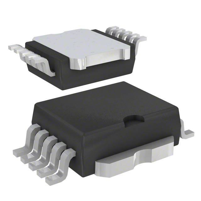
封装信息: - 提供了PowerSO-10™封装的详细信息,包括管式封装和卷带封装的订购代码。
VND600SPTR-E 价格&库存

很抱歉,暂时无法提供与“VND600SPTR-E”相匹配的价格&库存,您可以联系我们找货

免费人工找货