VND670SP
Dual high-side switch with dual Power MOSFET
gate driver (bridge configuration)
Features
Type
RDS(on)
IOUT
VCC
VND670SP
30mΩ(1)
15A(1)
40V
)
s
(
ct
10
1. Per each channel.
1
u
d
o
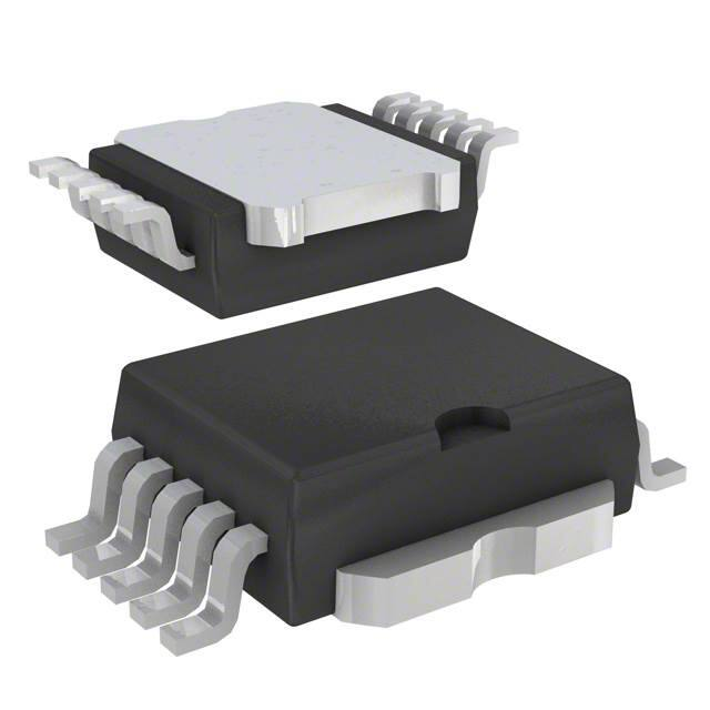
PowerSO-10
■
5V logic level compatible inputs
■
Gate drive for two external power MOSFET
■
Undervoltage and overvoltage shutdown
■
Overvoltage clamp
■
Thermal shutdown
■
Cross-conduction protection
■
Current limitation
■
Very low standby power consumption
■
PWM operation up to 10 KHz
■
Protection against loss of ground and loss of
VCC
■
Reverse battery protection
P
e
t
e
l
o
t
e
l
o
)
(s
t
c
u
d
o
r
r
P
e
Description
The VND670SP is a monolithic device made
using STMicroelectronics VIPower technology
M0-3, intended for driving motors in full bridge
configuration. The device integrates two 30 mW
Power MOSFET in high-side configuration, and
provides gate drive for two external Power
MOSFET used as low side switches. INA and INB
allow to select clockwise or counter clockwise
drive or brake; DIAGA/ENA, DIAGB/ENB allow to
disable one half bridge and feedback diagnostic.
Built-in thermal shutdown, combined with a
current limiter, protects the chip in
overtemperature and short circuit conditions.
Short to battery protects the external connected
low-side Power MOSFET.
s
b
O
s
b
O
Table 1.
Device summary
Order codes
Package
PowerSO-10
December 2008
Tube
Tape and reel
VND670SP
VND670SP13TR
Rev 2
1/20
www.st.com
20
�Contents
VND670SP
Contents
1
Block diagram and pin description . . . . . . . . . . . . . . . . . . . . . . . . . . . . . 5
2
Electrical specifications . . . . . . . . . . . . . . . . . . . . . . . . . . . . . . . . . . . . . . 6
3
2.1
Absolute maximum ratings . . . . . . . . . . . . . . . . . . . . . . . . . . . . . . . . . . . . . 6
2.2
Thermal data . . . . . . . . . . . . . . . . . . . . . . . . . . . . . . . . . . . . . . . . . . . . . . . 7
2.3
Electrical characteristics . . . . . . . . . . . . . . . . . . . . . . . . . . . . . . . . . . . . . . . 7
)
s
(
ct
4
Application information . . . . . . . . . . . . . . . . . . . . . . . . . . . . . . . . . . . . . 11
3.1
Normal operating conditions . . . . . . . . . . . . . . . . . . . . . . . . . . . . . . . . . . 12
3.2
Fault conditions . . . . . . . . . . . . . . . . . . . . . . . . . . . . . . . . . . . . . . . . . . . . 13
3.3
Test mode . . . . . . . . . . . . . . . . . . . . . . . . . . . . . . . . . . . . . . . . . . . . . . . . . 13
u
d
o
r
P
e
®
4.1
ECOPACK packages . . . . . . . . . . . . . . . . . . . . . . . . . . . . . . . . . . . . . . . 16
4.2
PowerSO-10 mechanical data . . . . . . . . . . . . . . . . . . . . . . . . . . . . . . . . . 16
4.3
PowerSO-10 packing information . . . . . . . . . . . . . . . . . . . . . . . . . . . . . . . 18
)
(s
t
c
u
5
s
b
O
Revision history . . . . . . . . . . . . . . . . . . . . . . . . . . . . . . . . . . . . . . . . . . . 19
d
o
r
P
e
t
e
l
o
s
b
O
2/20
t
e
l
o
Package and packing information . . . . . . . . . . . . . . . . . . . . . . . . . . . . . 16
�VND670SP
List of tables
List of tables
Table 1.
Table 2.
Table 3.
Table 4.
Table 5.
Table 6.
Table 7.
Table 8.
Table 9.
Table 10.
Table 11.
Table 12.
Table 13.
Table 14.
Table 15.
Device summary . . . . . . . . . . . . . . . . . . . . . . . . . . . . . . . . . . . . . . . . . . . . . . . . . . . . . . . . . . 1
Suggested connections for unused and not connected pins . . . . . . . . . . . . . . . . . . . . . . . . 5
Absolute maximum ratings . . . . . . . . . . . . . . . . . . . . . . . . . . . . . . . . . . . . . . . . . . . . . . . . . . 6
Thermal data (per island) . . . . . . . . . . . . . . . . . . . . . . . . . . . . . . . . . . . . . . . . . . . . . . . . . . . 7
Power . . . . . . . . . . . . . . . . . . . . . . . . . . . . . . . . . . . . . . . . . . . . . . . . . . . . . . . . . . . . . . . . . . 7
Switching . . . . . . . . . . . . . . . . . . . . . . . . . . . . . . . . . . . . . . . . . . . . . . . . . . . . . . . . . . . . . . . 7
Protection and diagnostic . . . . . . . . . . . . . . . . . . . . . . . . . . . . . . . . . . . . . . . . . . . . . . . . . . . 8
PWM . . . . . . . . . . . . . . . . . . . . . . . . . . . . . . . . . . . . . . . . . . . . . . . . . . . . . . . . . . . . . . . . . . . 8
Logic inputs. . . . . . . . . . . . . . . . . . . . . . . . . . . . . . . . . . . . . . . . . . . . . . . . . . . . . . . . . . . . . . 8
Enable. . . . . . . . . . . . . . . . . . . . . . . . . . . . . . . . . . . . . . . . . . . . . . . . . . . . . . . . . . . . . . . . . . 9
Truth table in normal operating conditions . . . . . . . . . . . . . . . . . . . . . . . . . . . . . . . . . . . . . 12
Truth table in fault conditions (detected on OUTA) . . . . . . . . . . . . . . . . . . . . . . . . . . . . . . . 13
Electrical transient requirements . . . . . . . . . . . . . . . . . . . . . . . . . . . . . . . . . . . . . . . . . . . . 14
PowerSO-10 mechanical data . . . . . . . . . . . . . . . . . . . . . . . . . . . . . . . . . . . . . . . . . . . . . . 17
Document revision history . . . . . . . . . . . . . . . . . . . . . . . . . . . . . . . . . . . . . . . . . . . . . . . . . 19
)
s
(
ct
u
d
o
r
P
e
t
e
l
o
)
(s
s
b
O
t
c
u
d
o
r
P
e
t
e
l
o
s
b
O
3/20
�List of figures
VND670SP
List of figures
Figure 1.
Figure 2.
Figure 3.
Figure 4.
Figure 5.
Figure 6.
Figure 7.
Figure 8.
Figure 9.
Figure 10.
Figure 11.
Figure 12.
Figure 13.
Figure 14.
Block diagram . . . . . . . . . . . . . . . . . . . . . . . . . . . . . . . . . . . . . . . . . . . . . . . . . . . . . . . . . . . . 5
Configuration diagram (top view) . . . . . . . . . . . . . . . . . . . . . . . . . . . . . . . . . . . . . . . . . . . . . 5
Current and voltage conventions . . . . . . . . . . . . . . . . . . . . . . . . . . . . . . . . . . . . . . . . . . . . . 6
Test conditions for high-side switching times measurement. . . . . . . . . . . . . . . . . . . . . . . . . 9
Test conditions for external Power MOSFET switching times measurement . . . . . . . . . . 10
Definition of the external Power MOSFET turn-on dead time tdel . . . . . . . . . . . . . . . . . . . 10
Typical application circuit for DC to 10 KHz PWM operation . . . . . . . . . . . . . . . . . . . . . . . 11
Typical application circuit for a 20 KHz PWM operation . . . . . . . . . . . . . . . . . . . . . . . . . . . 12
Waveforms (1) . . . . . . . . . . . . . . . . . . . . . . . . . . . . . . . . . . . . . . . . . . . . . . . . . . . . . . . . . . 14
Waveforms (2) . . . . . . . . . . . . . . . . . . . . . . . . . . . . . . . . . . . . . . . . . . . . . . . . . . . . . . . . . . 15
PowerSO-10 package dimensions . . . . . . . . . . . . . . . . . . . . . . . . . . . . . . . . . . . . . . . . . . . 16
PowerSO-10 suggested pad layout . . . . . . . . . . . . . . . . . . . . . . . . . . . . . . . . . . . . . . . . . . 18
PowerSO-10 tube shipment (no suffix) . . . . . . . . . . . . . . . . . . . . . . . . . . . . . . . . . . . . . . . . 18
SO-28 tape and reel shipment (suffix “TR”) . . . . . . . . . . . . . . . . . . . . . . . . . . . . . . . . . . . . 18
)
s
(
ct
u
d
o
r
P
e
t
e
l
o
)
(s
t
c
u
d
o
r
P
e
t
e
l
o
s
b
O
4/20
s
b
O
�VND670SP
1
Block diagram and pin description
Block diagram and pin description
Figure 1.
Block diagram
VCC
Undervolt.
INTERNAL
SUPPLY
INA
OUTA
Short to battery
INB
)
s
(
ct
LOGIC
DIAGA/ENA
DIAGB/ENB
PWM
Overtemp.
A
e
t
e
l
Current
Limiter B
Overtemp.
B
o
s
b
Figure 2.
GATEA
Current
Limiter A
GATEB
GND
O
)
s
(
t
c
Pr
O
OUTPUT B
GATE B
GROUND
GATE A
OUTPUT A
5
4
3
6
7
8
9
10
INPUT B
DIAGB/ENB
PWM
DIAGA/ENA
INPUT A
bs
Pr
Configuration diagram (top view)
u
d
o
e
t
e
ol
OUTB
u
d
o
Short to battery
2
1
11
VCC
Table 2.
Suggested connections for unused and not connected pins
Connection / pin
Status
N.C.
Output
Input
Floating
X
X
X
X
To ground
X
Through 10KΩ
resistor
5/20
�Electrical specifications
2
VND670SP
Electrical specifications
Figure 3.
Current and voltage conventions
ICC
VCC
IINA
VCC
INA
IINB
IENA
IENB
IOUTA
OUTA
IOUTB
INB
OUTB
DIAGA/ENA
GATEA
DIAGB/ENB
GATEB
IgsB
VOUTB
VgsB
Ipw
VINA VINB VENA VENB
2.1
IGND
Vpw
)
s
(
ct
VgsA
GND
PWM
VOUTA
IgsA
u
d
o
r
P
e
t
e
l
o
s
b
O
Absolute maximum ratings
Stressing the device above the rating listed in the “Absolute maximum ratings” table may
cause permanent damage to the device. These are stress ratings only and operation of the
device at these or any other conditions above those indicated in the Operating sections of
this specification is not implied. Exposure to Absolute Maximum Rating conditions for
extended periods may affect device reliability. Refer also to the STMicroelectronics SURE
Program and other relevant quality document.
)
(s
t
c
u
Table 3.
d
o
r
P
e
Symbol
t
e
l
o
s
b
O
Parameter
Value
Unit
-0.3..40
V
VCC
Supply voltage
Imax1
Maximum output current (continuous)
15
A
Imax2
Maximum output current (250ms pulse duration)
20
A
- 15
A
IR
Reverse DC output current
IIN
Input current
+/- 10
mA
IEN
Enable pin current
+/- 10
mA
Ipw
PWM pin current
+/- 10
mA
Igs
Output gate current
+/- 20
mA
Electrostatic discharge ( R = 1.5KΩ; C = 100pF)
2000
V
Junction operating temperature
- 40 to 150
°C
Storage temperature
- 55 to 150
°C
VESD
Tj
Tstg
6/20
Absolute maximum ratings
�VND670SP
2.2
Electrical specifications
Thermal data
Table 4.
Thermal data (per island)
Symbol
Parameter
Rthj-case
Thermal resistance junction-case
Rthj-amb
Thermal resistance junction-ambient
Max. value
Unit
1.4
°C/W
50(1)
°C/W
1. When mounted using the recommended pad size on FR-4 board (see AN515 Application Note).
2.3
Electrical characteristics
)
s
(
ct
Values specified in this section are for 9V < VCC < 18V; -40°C < Tj < 150°C, unless
otherwise stated.
Table 5.
Symbol
Parameter
VCC
Operating supply voltage
RON
On-state resistance
Is
Supply current
)
(s
Vgs,cl
Gate output clamp voltage
d
o
r
P
e
s
b
O
t
c
u
e
t
e
ol
ILOAD = 12A
ILOAD = 12A
Tj = 25°C
s
b
O
Gate output voltage
Table 6.
t
e
l
o
Test conditions
Vgate
Symbol
u
d
o
Power
Pr
Min.
Typ.
5.5
26
On-state
Off-state
Igs= - 1 mA
5.0
Max.
Unit
36
V
50
30
mΩ
mΩ
15
40
mA
µA
8.5
V
6.0
6.8
8.0
V
Min.
Typ.
Max.
Unit
Switching (VCC = 13V, RLOAD = 1.1Ω)
Parameter
Test conditions
tD(on)
Turn-on delay time
50
150
µs
tD(off)
Turn-off delay time
45
135
µs
50
150
µs
40
120
µs
tr
Output voltage rise time
tf
Output voltage fall time
Input rise time < 1µs
(see Figure 4)
(dVOUT/dt)on
Turn-on voltage slope
160
500
V/ ms
(dVOUT/dt)off
Turn-off voltage slope
230
1200
V/ ms
tdong
Vgsturn-on delay time
0.5
2
µs
2.6
10
µs
1.0
5.0
µs
2.2
10
µs
600
1800
µs
trg
tdoffg
Vgs rise time
Vgsturn-off delay time
tfg
Vgs fall time
tdel
External MOSFET
turn-on dead time
C1=4.7nF
Break to ground
configuration
(see Figure 5)
(see Figure 6)
7/20
�Electrical specifications
Table 7.
VND670SP
Protection and diagnostic
Symbol
Parameter
VUSD
Undervoltage shutdown
VOV
Overvoltage shutdown
36
43
V
ILIM
Current limitation
30
45
A
TTSD
Thermal shutdown
temperature
VIN = 3.25 V
150
170
Vocl
Output turn-off clamp
voltage
ILOAD = 12A, L = 6mH
VCC55
Vsat
External MOSFET
saturation voltage
detection threshold
Table 8.
Symbol
Parameter
Vpwl
PWM low level voltage
Ipwl
PWM pin current
Ipwh
PWM pin current
Vpwhhyst
PWM hysteresis
voltage
t
e
l
o
Table 9.
Symbol
s
(
t
c
u
d
o
Ipw = 1 mA
Ipw = -1 mA
Test mode PWM pin
voltage
Test mode PWM pin
current
Vpwtest = -2.0 V
Unit
5.5
V
200
°C
VCC41
V
)
s
(
t
5.5
Typ.
V
Max.
Unit
1.5
V
1
µA
3.25
V
10
0.5
µA
V
VCC+0.3
-5.0
VCC+0.7
-3.5
VCC+1.0
-2.0
V
V
-3.5
-2.0
-0.5
V
-2000
-500
µA
Logic inputs
Parameter
Input low level voltage
IINL
Input current
VIH
Input high level voltage
IINH
Input current
VICL
8/20
)-
VIL
VIHYST
o
r
P
Vpw = 3.25V
PWM clamp voltage
r
P
e
Ipwtest
s
b
O
4.2
Max.
c
u
d
Min.
ete
ol
Vpw = 1.5V
PWM high level voltage
Typ.
2.5
Test conditions
Vpwh
Vpwtest
Min.
PWM
Vpwcl
s
b
O
Test conditions
Test conditions
VIN = 1.5 V
Typ.
Max.
Unit
1.5
V
1
µA
3.25
V
VIN = 3.25 V
Input hysteresis voltage
Input clamp voltage
Min.
10
0.5
IIN=1mA
IIN=-1mA
6.0
-1.0
µA
V
6.8
-0.7
8.0
-0.3
V
V
�VND670SP
Electrical specifications
Table 10.
Enable
Symbol
Parameter
Min.
VENL
Enable low level voltage
Normal operation
(DIAGX/ENX pin acts
as an input pin)
IENL
Enable pin current
VEN = 1.5 V
VENH
Enable high level voltage
Normal operation
(DIAGX/ENX pin acts
as an input pin)
IENH
Enable pin current
VEN = 3.25 V
VEHYST
Enable hysteresis voltage
Normal operation
(DIAGX/ENX pin acts
as an input pin)
0.5
VENCL
Enable clamp voltage
IEN = 1mA
IEN = -1mA
6.0
-1.0
Enable output low level
voltage
Fault operation
(DIAGX/ENX pin acts
as an input pin)
IEN = 1.6 mA
VDIAG
Figure 4.
Typ.
O
)
Max.
Unit
1.5
V
1
µA
3.25
V
10
µA
)
s
(
ct
V
r
P
e
u
d
o
6.8
-0.7
let
o
s
b
8.0
-0.3
V
V
0.4
V
Test conditions for high-side switching times measurement
s
(
t
c
VOUTA, B
u
d
o
r
P
e
90%
80%
(dVOUT/dt)off
(dVOUT/dt)on
10%
t
e
l
o
s
b
O
Test conditions
VINA, B
t
td(on) tr
td(off) tf
t
9/20
�Electrical specifications
Figure 5.
VND670SP
Test conditions for external Power MOSFET switching times
measurement
VgsA, B
90%
80%
20%
10%
Vpw
tdong
tdoffg
trg
t
)
s
(
ct
tfg
u
d
o
r
P
e
Figure 6.
t
e
l
o
s
b
O
Definition of the external Power MOSFET turn-on dead time tdel
)
(s
INA
t
c
u
d
o
r
INB
P
e
let
o
s
b
O
OUTA
VgsA
tdel
10/20
t
�VND670SP
3
Application information
Application information
Figure 7.
Typical application circuit for DC to 10 KHz PWM operation
+5V
+5V
R1
R1
VCC
Rprot
Rprot
1K
1K
DIAGB/ENB
DIAGA/ENA
VND670SP
Rprot
1K
GND
OUTA
PWM
)
s
(
ct
OUTB
Rgnd(*)
du
Rprot
1K
INA
GATEA
UP
e
t
e
DOWN l
o
s
b
-O
M
External Power Mos A
Note:
)
s
(
ct
o
r
P
GATEB
INB
Rprot
1K
External Power Mos B
1
Reverse battery protection: series relay in VCC line: Rgnd=0 Ohms; series fuse in VCC line
with antiparallel diode between ground and VCC: Rgnd=10 Ohms.
2
Layout hints: the connection between GND pin of the VN670SP and the Power MOSFET
SOURCE connections should be kept short enough to ensure that the dynamic difference
between these two points never exceed 1V for the bridge to operate properly.
u
d
o
r
P
e
t
e
l
o
s
b
O
11/20
�Application information
Figure 8.
VND670SP
Typical application circuit for a 20 KHz PWM operation
+5V
+5V
R1
R1
VCC
Rprot
Rprot
1K
1K
DIAGB/ENB
DIAGA/ENA
VND670SP
Rprot
1K
OUTA
INA
OUTB
Rgnd(*)
Rprot
Rprot
1K
PWM
UP
GATEA
D1
u
d
o
D2
r
P
e
DOWN
27Ω
Note:
1
Note:
t
e
l
o
External
Power Mos B
s
b
O
Table 11.
s
b
O
27Ω
Reverse battery protection: series relay in VCC line: Rgnd = 0 Ohms; series fuse in VCC line
with antiparallel diode between ground and VCC: Rgnd=10 Ohms.
)
s
Normal operatingt(
conditions
c
u
d
o
r
P
e
t
e
ol
3.1
)
s
(
ct
GATEB
M
External
Power Mos A
1K
INB
Truth table in normal operating conditions
INA
INB
DIAGA/ENA
DIAGB/ENB
OUTA
OUTB
GATEA
GATEB
Comment
1
1
1
1
H
H
L
L
Brake to VCC
1
0
1
1
H
L
L
H
Clockwise
0
1
1
1
L
H
H
L
Counter cw
0
0
1
1
L
L
H
H
Brake to GND
X
X
0
0
L
L
L
L
Stand by
1
X
1
0
H
L
L
L
HSA only
0
X
1
0
L
L
H
L
MOSA only
X
1
0
1
L
H
L
L
HSB only
X
0
0
1
L
L
L
H
MOSB only
1
In normal operating conditions the DIAGX/ENX pin is considered as an input pin by the
device. This pin must be externally pulled high.
2
PWM pin usage:
In all cases, a “0” on the PWM pin will turn-off both GATEA and GATEB outputs. When PWM
rises back to “1”, GATEA or GATEB turn on again depending on the input pin state.
12/20
�VND670SP
3.2
Application information
Fault conditions
In case of a fault conditions the DIAGX/ENX pin is considered as an output pin by the device.
The fault conditions are:
●
overtemperature on one or both high-sides;
●
short to battery condition on the output (saturation detection on the external connected
Power MOSFET).
Possible origins of fault conditions may be:
●
OUTA is shorted to ground ---> overtemperature detection on high-side A.
●
OUTA is shorted to VCC ---> external Power MOSFET saturation detection (driven by
GATEA).
)
s
(
ct
When a fault condition is detected, the user can know which power element is in fault by
monitoring the INA, INB, DIAGA/ENA and DIAGB/ENB pins.
u
d
o
In any case, when a fault is detected, the faulty half bridge is latched off. To turn-on the
respective output (GATEX or OUTX) again, the input signal must rise from low to high level.
Table 12.
INA
INB
DIAGA/ENA
DIAGB/ENB
OUTA
OUTB
GATEA
GATEB
1
1
0
1
Open
H
L
L
1
0
0
1
Open
Open
L
L
0
1
0
1
Open
H
L
L
0
0
0
1
Open
Open
L
L
X
X
0
0
Open
Open
L
L
1
X
0
0
Open
Open
L
L
0
X
0
Open
Open
L
L
X
1
0
1
Open
H
L
L
0
1
Open
Open
L
L
ro
0
t
e
l
o
bs
O
)
t(s
c
u
d
0
P
e
X
3.3
r
P
e
Truth table in fault conditions (detected on OUTA)
s
b
O
t
e
Test mode
l
o
The PWM pin allows to test the load connection between two half-bridges. In the test mode
(Vpwm=-2V) the external Power Mos gate drivers are disabled. The INA or INB inputs allow to
turn-on the high-side A or B, respectively, in order to connect one side of the load at VCC
voltage. The check of the voltage on the other side of the load allow to verify the continuity of
the load connection. In case of load disconnection the DIADX/ENX pin corresponding to the
faulty output is pulled down.
13/20
�Application information
Table 13.
VND670SP
Electrical transient requirements
ISO T/R
Test level
7637/1
Test pulse
I
II
III
IV
1
- 25V(1)
- 50V(1)
- 75V(1)
- 100V(1)
2
25V(1)
(1)
(1)
(1)
0.2ms, 10Ω
(1)
+
+ 50V
(1)
(1)
+ 75V
Delays and impedance
2ms, 10Ω
+ 100V
(1)
3a
- 25V
- 50V
- 100V
- 150V
0.1µs, 50Ω
3b
+ 25V(1)
+ 50V(1)
+ 75V(1)
+ 100V(1)
0.1µs, 50Ω
4
-
4V(1)
(1)
- 5V
(1)
5
(2)
+ 46.5V
+ 26.5V
(1)
(1)
- 6V
+ 66.5V
- 7V
(2)
+ 86.5V
100ms, 0.01Ω
(2)
)
s
(
ct
400ms, 2Ω
1. All functions of the device are performed as designed after exposure to disturbance.
2. One or more functions of the device is not performed as designed after exposure and cannot be returned to
proper operation without replacing the device.
Figure 9.
u
d
o
r
P
e
Waveforms (1)
t
e
l
o
OUTA shorted to VCC and undervoltage shutdown
INA
INB
OUTA
OUTB
)
(s
GATEA
GATEB
t
c
u
DIAGB/ENB
DIAGA/ENA
od
let
r
P
e
o
s
b
O
normal operation
s
b
O
OUTA shorted to VCC
normal operation
undervoltage shutdown
Load disconnection test (INA=1, PWM=-2V)
INA
INB
PWM
(test mode)
OUTA
OUTB
GATEA
GATEB
DIAGA/ENA
DIAGB/ENB
load connected
14/20
load disconnected
load connected back
�VND670SP
Application information
Figure 10. Waveforms (2)
NORMAL OPERATION (DIAGA/ENA=1, DIAGB/ENB=1)
DIAGA/ENA
DIAGB/ENB
INA
INB
PWM
OUTA
OUTB
GATEA
GATEB
NORMAL OPERATION (DIAGA/ENA=1, DIAGB/ENB=0 and DIAGA/ENA=0, DIAGB/ENB=1)
)
s
(
ct
DIAGA/ENA
DIAGB/ENB
u
d
o
INA
INB
PWM
r
P
e
OUTA
OUTB
GATEA
t
e
l
o
GATEB
s
b
O
CURRENT LIMITATION/THERMAL SHUTDOWN or OUTA SHORTED TO GROUND
)
(s
INA
INB
ILIM
ct
IOUTA
Tj
u
d
o
TTSD
r
P
e
DIAGA/ENA
DIAGB/ENB
let
o
s
b
GATEA
GATEB
normal operation
OUTA shorted to ground
normal operation
O
15/20
�Package and packing information
VND670SP
4
Package and packing information
4.1
ECOPACK® packages
In order to meet environmental requirements, ST offers these devices in different grades of
ECOPACK® packages, depending on their level of environmental compliance. ECOPACK®
specifications, grade definitions and product status are available at: www.st.com.
ECOPACK® is an ST trademark.
4.2
PowerSO-10 mechanical data
)
s
(
ct
Figure 11. PowerSO-10 package dimensions
u
d
o
B
r
P
e
0.10 A B
10
H
E
1
)
(s
e
B
0.25
h
F
t
e
l
o
s
b
O
16/20
E
s
b
O
DETAIL "A"
D
= D1 =
=
=
E4
S EATING
P LANE
A
C
t
c
u
od
r
P
e
A
t
e
l
o
E2
S EATING
PLANE
A1
A1
L
DETAIL "A"
α
�VND670SP
Package and packing information
Table 14.
PowerSO-10 mechanical data
mm
Dim.
Min.
3.35
3.65
A(1)
3.4
3.6
A1
0
0.10
B
0.40
0.60
B(1)
0.37
0.53
C
0.35
(1)
0.23
D
9.40
D1
7.40
E
9.30
E2
7.20
E2(1)
7.30
E4
5.90
(s)
E4(1)
ct
du
F
u
d
o
ete
bs
ol
Pr
0.32
9.60
7.60
9.50
7.60
7.50
-O
6.10
6.30
1.27
1.25
1.35
1.20
1.40
H
13.80
14.40
H(1)
13.85
14.35
o
r
P
F(1)
b
O
)
s
(
ct
0.55
5.90
e
so
Max.
A
C
e
t
e
l
Typ.
h
0.50
L
1.20
1.80
L(1)
0.80
1.10
α
0°
8°
α(1)
2°
8°
1. Muar only POA P013P.
17/20
�Package and packing information
4.3
VND670SP
PowerSO-10 packing information
Figure 12. PowerSO-10 suggested Figure 13. PowerSO-10 tube shipment
pad layout
(no suffix)
14.6 - 14.9
CASABLANCA
B
10.8 - 11
MUAR
C
6.30
C
A
A
0.67 - 0.73
1
9.5
10
9
8
2
3
All dimensions are in mm.
7
4
5
B
0.54 - 0.6
1.27
6
Base Q.ty Bulk Q.ty
Casablanca
Muar
50
50
1000
1000
Tube length (±
0.5)
532
532
)
(s
b
O
B
10.4 16.4
4.9 17.2
C (±
0.1)
0.8
0.8
u
d
o
r
P
e
Figure 14. PowerSO-10 tape and reel shipment (suffix “TR”)
let
so
)
s
(
ct
A
Reel dimensions
Base Q.ty
Bulk Q.ty
A (max)
B (min)
C (± 0.2)
F
G (+ 2 / -0)
N (min)
T (max)
t
c
u
600
600
330
1.5
13
20.2
24.4
60
30.4
d
o
r
P
e
Tape dimensions
According to Electronic Industries Association
(EIA) Standard 481 rev. A, Feb. 1986
t
e
l
o
s
b
O
Tape width
Tape Hole Spacing
Component Spacing
Hole Diameter
Hole Diameter
Hole Position
Compartment Depth
Hole Spacing
W
P0 (± 0.1)
P
D (± 0.1/-0)
D1 (min)
F (± 0.05)
K (max)
P1 (± 0.1)
All dimensions are in mm.
24
4
24
1.5
1.5
11.5
6.5
2
End
Start
Top
cover
tape
No components
Components
500mm min
Empty components pockets
saled with cover tape.
User direction of feed
18/20
No components
500mm min
�VND670SP
5
Revision history
Revision history
Table 15.
Document revision history
Date
Revision
03-May-2006
1
Initial release.
2
Document reformatted and restructured.
Added contents, list of tables and figures.
Added ECOPACK® packages information.
11-Dec-2008
Changes
)
s
(
ct
u
d
o
r
P
e
t
e
l
o
)
(s
s
b
O
t
c
u
d
o
r
P
e
t
e
l
o
s
b
O
19/20
�VND670SP
)
s
(
ct
Please Read Carefully:
u
d
o
Information in this document is provided solely in connection with ST products. STMicroelectronics NV and its subsidiaries (“ST”) reserve the
right to make changes, corrections, modifications or improvements, to this document, and the products and services described herein at any
time, without notice.
r
P
e
All ST products are sold pursuant to ST’s terms and conditions of sale.
Purchasers are solely responsible for the choice, selection and use of the ST products and services described herein, and ST assumes no
liability whatsoever relating to the choice, selection or use of the ST products and services described herein.
t
e
l
o
No license, express or implied, by estoppel or otherwise, to any intellectual property rights is granted under this document. If any part of this
document refers to any third party products or services it shall not be deemed a license grant by ST for the use of such third party products
or services, or any intellectual property contained therein or considered as a warranty covering the use in any manner whatsoever of such
third party products or services or any intellectual property contained therein.
)
(s
s
b
O
UNLESS OTHERWISE SET FORTH IN ST’S TERMS AND CONDITIONS OF SALE ST DISCLAIMS ANY EXPRESS OR IMPLIED
WARRANTY WITH RESPECT TO THE USE AND/OR SALE OF ST PRODUCTS INCLUDING WITHOUT LIMITATION IMPLIED
WARRANTIES OF MERCHANTABILITY, FITNESS FOR A PARTICULAR PURPOSE (AND THEIR EQUIVALENTS UNDER THE LAWS
OF ANY JURISDICTION), OR INFRINGEMENT OF ANY PATENT, COPYRIGHT OR OTHER INTELLECTUAL PROPERTY RIGHT.
t
c
u
UNLESS EXPRESSLY APPROVED IN WRITING BY AN AUTHORIZED ST REPRESENTATIVE, ST PRODUCTS ARE NOT
RECOMMENDED, AUTHORIZED OR WARRANTED FOR USE IN MILITARY, AIR CRAFT, SPACE, LIFE SAVING, OR LIFE SUSTAINING
APPLICATIONS, NOR IN PRODUCTS OR SYSTEMS WHERE FAILURE OR MALFUNCTION MAY RESULT IN PERSONAL INJURY,
DEATH, OR SEVERE PROPERTY OR ENVIRONMENTAL DAMAGE. ST PRODUCTS WHICH ARE NOT SPECIFIED AS "AUTOMOTIVE
GRADE" MAY ONLY BE USED IN AUTOMOTIVE APPLICATIONS AT USER’S OWN RISK.
d
o
r
P
e
t
e
l
o
Resale of ST products with provisions different from the statements and/or technical features set forth in this document shall immediately void
any warranty granted by ST for the ST product or service described herein and shall not create or extend in any manner whatsoever, any
liability of ST.
s
b
O
ST and the ST logo are trademarks or registered trademarks of ST in various countries.
Information in this document supersedes and replaces all information previously supplied.
The ST logo is a registered trademark of STMicroelectronics. All other names are the property of their respective owners.
© 2008 STMicroelectronics - All rights reserved
STMicroelectronics group of companies
Australia - Belgium - Brazil - Canada - China - Czech Republic - Finland - France - Germany - Hong Kong - India - Israel - Italy - Japan Malaysia - Malta - Morocco - Singapore - Spain - Sweden - Switzerland - United Kingdom - United States of America
www.st.com
20/20
�