VNP49N04
OMNIFET :
FULLY AUTOPROTECTED POWER MOSFET
TYPE
VNP49N04
■
■
■
■
■
■
■
■
■
■
V clamp
R DS(on)
I l im
42 V
0.02 W
49 A
LINEAR CURRENT LIMITATION
THERMAL SHUT DOWN
SHORT CIRCUIT PROTECTION
INTEGRATED CLAMP
LOW CURRENT DRAWN FROM INPUT PIN
DIAGNOSTIC FEEDBACK THROUGH INPUT
PIN
ESD PROTECTION
DIRECT ACCESS TO THE GATE OF THE
POWER MOSFET (ANALOG DRIVING)
COMPATIBLE WITH STANDARD POWER
MOSFET
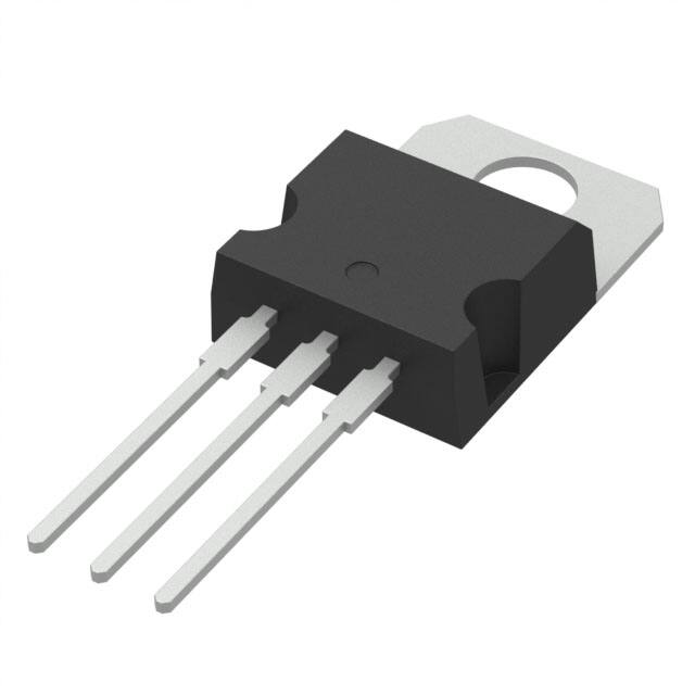
STANDARD TO-220 PACKAGE
DESCRIPTION
The VNP49N04 is a monolithic device made
using STMicroelectronics VIPower Technology,
intended for replacement of standard power
MOSFETS in DC to 50 KHz applications.
Built-in thermal shut-down, linear current limita-
1
2
3
TO-220
tion and overvoltage clamp protect the chip in
harsh enviroments.
Fault feedback can be detected by monitoring the
voltage at the input pin.
BLOCK DIAGRAM
March 2004
1/11
�VNP49N04
ABSOLUTE MAXIMUM RATING
Symbol
Parameter
Value
Unit
V DS
Drain-source Voltage (V in = 0)
Internally Clamped
V
V in
Input Voltage
18
V
ID
Drain Current
Internally Limited
A
IR
Reverse DC O utput Current
-50
A
V esd
Electrostatic Discharge (C= 100 pF , R=1.5 KW)
2000
V
P to t
Total Dissipation at T c = 25 o C
125
W
Tj
Tc
T st g
Operating Junction T emperature
Case Operating T emperature
Internally Limited
o
C
Internally Limited
o
C
-55 to 150
o
C
Storage Temperature
THERMAL DATA
R t hj-ca se
R t hj- amb
Thermal Resistance Junction-case
Thermal Resistance Junction-ambient
Max
Max
o
1
62.5
o
C/W
C/W
ELECTRICAL CHARACTERISTICS (Tcase = 25 oC unless otherwise specified)
OFF
Symb ol
Parameter
Test Cond ition s
V CLAMP
Drain-source Clamp
Voltage
I D = 200 mA
V CL TH
Drain-source Clamp
Threshold Voltage
I D = 2 mA
V I NCL
Input-Source Reverse
Clamp Voltage
I in = -1 mA
I DSS
Zero Input Voltage
Drain Current (V in = 0)
V DS = 13 V
V DS = 25 V
V in = 0
V in = 0
I I SS
Supply Current from
Input Pin
V DS = 0 V
Vin = 10 V
V in = 0
V in = 0
Min.
Typ .
Max.
Un it
36
42
48
V
35
V
-1
-0.3
V
50
200
mA
mA
250
500
mA
Typ .
Max.
Un it
3
V
0.02
0.025
W
W
Max.
Un it
ON (*)
Symb ol
Parameter
Test Cond ition s
Min.
0.8
V IN(th)
Input Threshold
Voltage
V DS = Vin
ID +I in = 1 mA
R DS( on)
Static Drain-source On
Resistance
V i n = 10 V
Vi n = 5 V
I D = 25 A
ID = 25 A
DYNAMIC
Symb ol
g fs (*)
C oss
2/11
Parameter
Test Cond ition s
Forward
Transconductance
V DS = 13 V
I D = 25 A
Output Capacitance
V DS = 13 V
f = 1 MHz
Vin = 0
Min.
Typ .
25
30
1100
S
1500
pF
�VNP49N04
ELECTRICAL CHARACTERISTICS (continued)
SWITCHING (**)
Symb ol
Parameter
Test Cond ition s
t d(on)
tr
t d(of f)
tf
Turn-on Delay Time
Rise Time
Turn-off Delay Time
Fall T ime
V DD = 15 V
V gen = 10 V
(see figure 3)
Id = 25 A
R gen = 10 W
t d(on)
tr
t d(of f)
tf
Turn-on Delay Time
Rise Time
Turn-off Delay Time
Fall T ime
V DD = 15 V
V gen = 10 V
(see figure 3)
Id = 25 A
R gen = 1000 W
Turn-on Current Slope
V DD = 15 V
V i n = 10 V
Total Input Charge
V DD = 15 V
(di/dt) on
Qi
Min.
ID = 25 A
R gen = 10 W
ID = 25 A
V i n = 10 V
Typ .
Max.
Un it
200
1300
800
300
300
1800
1200
450
ns
ns
ns
ns
1.3
3.8
12
6.1
1.9
5.2
14
8.5
ms
ms
ms
ms
25
A/ms
100
nC
SOURCE DRAIN DIODE
Symb ol
Parameter
Test Cond ition s
V SD (*)
Forward O n Voltage
I SD = 25 A
t r r (**)
Reverse Recovery
Time
Reverse Recovery
Charge
Reverse Recovery
Current
I SD = 25 A
di/dt = 100 A/ms
V DD = 30 V
Tj = 25 oC
(see test circuit, figure 5)
Q r r (**)
I RRM (**)
Min.
Typ .
V in = 0
Max.
Un it
1.6
V
250
ns
910
nC
7.5
A
PROTECTION
Symb ol
I lim
Parameter
Test Cond ition s
Min.
Typ .
Max.
Un it
VDS = 13 V
V DS = 13 V
30
30
49
49
68
68
A
A
35
90
50
150
ms
ms
Drain Current Limit
V i n = 10 V
Vi n = 5 V
t dl im (**)
Step Response
Current Limit
V i n = 10 V
Vi n = 5 V
T jsh (**)
Overtemperature
Shutdown
150
o
C
T j rs (**)
Overtemperature Reset
135
o
C
I gf (**)
Fault Sink Current
V i n = 10 V
Vi n = 5 V
E as (**)
Single Pulse
Avalanche Energy
starting T j = 25 o C
V DD = 20 V
V i n = 10 V R gen = 1 KW L = 6 mH
50
20
VDS = 13 V
V DS = 13 V
4
mA
mA
J
(*) Pulsed: Pulse duration = 300 ms, duty cycle 1.5 %
(**) Parameters guaranteed by design/characterization
3/11
�VNP49N04
PROTECTION FEATURES
During normal operation, the Input pin is
electrically connected to the gate of the internal
power MOSFET. The device then behaves like a
standard power MOSFET and can be used as a
switch from DC to 50 KHz. The only difference
from the user s standpoint is that a small DC
current (Iiss) flows into the Input pin in order to
supply the internal circuitry.
The device integrates:
- OVERVOLTAGE
CLAMP
PROTECTION:
internally set at 42V, along with the rugged
avalanche characteristics of the Power
MOSFET stage give this device unrivalled
ruggedness and energy handling capability.
This feature is mainly important when driving
inductive loads.
- LINEAR CURRENT LIMITER CIRCUIT: limits
the drain current Id to Ilim whatever the Input
pin voltage. When the current limiter is active,
the device operates in the linear region, so
power dissipation may exceed the capability of
the heatsink. Both case and junction
temperatures increase, and if this phase lasts
long enough, junction temperature may reach
the overtemperature threshold Tjsh.
4/11
- OVERTEMPERATURE AND SHORT CIRCUIT
PROTECTION: these are based on sensing
the chip temperature and are not dependent on
the input voltage. The location of the sensing
element on the chip in the power stage area
ensures fast, accurate detection of the junction
temperature. Overtemperature cutout occurs at
minimum 150oC. The device is automatically
restarted when the chip temperature falls
below 135oC.
- STATUS FEEDBACK: In the case of an
overtemperature fault condition, a Status
Feedback is provided through the Input pin.
The internal protection circuit disconnects the
input from the gate and connects it instead to
ground via an equivalent resistance of 100 W.
The failure can be detected by monitoring the
voltage at the Input pin, which will be close to
ground potential.
Additional features of this device are ESD
protection according to the Human Body model
and the ability to be driven from a TTL Logic
circuit (with a small increase in RDS(on)).
�VNP49N04
Thermal Impedance
Derating Curve
Output Characteristics
Transconductance
Static Drain-Source On Resistance vs Input
Voltage
Static Drain-Source On Resistance
5/11
�VNP49N04
Static Drain-Source On Resistance
Input Charge vs Input Voltage
Capacitance Variations
Normalized Input Threshold Voltage vs
Temperature
Normalized On Resistance vs Temperature
Normalized On Resistance vs Temperature
6/11
�VNP49N04
Turn-on Current Slope
Turn-on Current Slope
Turn-off Drain-Source Voltage Slope
Turn-off Drain-Source Voltage Slope
Switching Time Resistive Load
Switching Time Resistive Load
7/11
�VNP49N04
Switching Time Resistive Load
Current Limit vs Junction Temperature
Step Response Current Limit
Source Drain Diode Forward Characteristics
8/11
�VNP49N04
Fig. 1: Unclamped Inductive Load Test Circuits
Fig. 2: Unclamped Inductive Waveforms
Fig. 3: Switching Times Test Circuits For
Resistive Load
Fig. 4: Input Charge Test Circuit
Fig. 5: Test Circuit For Inductive Load Switching
And Diode Recovery Times
Fig. 6: Waveforms
9/11
�VNP49N04
TO-220 MECHANICAL DATA
mm.
DIM.
MIN.
MAX.
A
4.40
4.60
b
0.61
0.88
b1
1.15
1.70
c
0.49
0.70
D
15.25
15.75
E
10
10.40
e
2.40
2.70
e1
4.95
5.15
F
1.23
1.32
H1
6.20
6.60
J1
2.40
2.72
L
13
14
L1
3.50
3.93
L20
16.40
L30
28.90
∅P
3.75
3.85
Q
2.65
2.95
Package Weight
10/11
TYP
1.9Gr. (Typ.)
�VNP49N04
Information furnished is believed to be accurate and reliable. However, STMicroelectronics assumes no responsibility for the consequences
of use of such information nor for any infringement of patents or other rights of third parties which may results from its use. No license is
granted by implication or otherwise under any patent or patent rights of STMicroelectronics. Specifications mentioned in this publication are
subject to change without notice. This publication supersedes and replaces all information previously supplied. STMicroelectronics products
are not authorized for use as critical components in life support devices or systems without express written approval of STMicroelectronics.
The ST logo is a trademark of STMicroelectronics
2004 STMicroelectronics - Printed in ITALY- All Rights Reserved.
STMicroelectronics GROUP OF COMPANIES
Australia - Brazil - Canada - China - Finland - France - Germany - Hong Kong - India - Israel - Italy - Japan - Malaysia Malta - Morocco - Singapore - Spain - Sweden - Switzerland - United Kingdom - U.S.A.
http://www.st.com
11/11
�
很抱歉,暂时无法提供与“VNP49N04-E”相匹配的价格&库存,您可以联系我们找货
免费人工找货