VNQ500
Quad channel high-side driver
Features
Max supply voltage
VCC
41V
Operating voltage range
VCC
5.5 to 36V
Max on-state resistance
RON
500mΩ
Current limitation (typ)
ILIM
0.4A
Off-state supply current
IS
25 µA
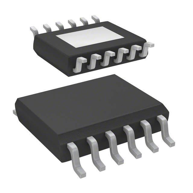
PowerSSO-12
Description
■
CMOS compatible I/O’s
■
Chip Enable
■
Junction over temperature protection and
diagnostic
■
Current limitation
■
Shorted load protection
■
Undervoltage shutdown
■
Protection against loss of ground
■
Very low standby current
■
In compliance with the 2002/95/EC european
directive
Table 1.
The VNQ500 is a monolithic device designed in
STMicroelectronics VIPower M0-3 technology,
intended for driving any kind of load with one side
connected to ground.
Active current limitation, combined with latched
thermal shutdown, protect the device against
overload.
In the case of over temperature of one channel
the relative I/O pin is pulled down.
The device automatically turns off in the case of
ground pin disconnection.
Device summary
Order codes
Package
PowerSSO-12
September 2013
Tube
Tape and reel
VNQ500PEP-E
VNQ500PEPTR-E
Doc ID 9934 Rev 4
1/24
www.st.com
1
�Contents
VNQ500
Contents
1
Block diagram and pin description . . . . . . . . . . . . . . . . . . . . . . . . . . . . . 5
2
Electrical specifications . . . . . . . . . . . . . . . . . . . . . . . . . . . . . . . . . . . . . . 7
3
2.1
Absolute maximum ratings . . . . . . . . . . . . . . . . . . . . . . . . . . . . . . . . . . . . . 7
2.2
Thermal data . . . . . . . . . . . . . . . . . . . . . . . . . . . . . . . . . . . . . . . . . . . . . . . 7
2.3
Electrical characteristics . . . . . . . . . . . . . . . . . . . . . . . . . . . . . . . . . . . . . . . 8
2.4
Electrical characteristics curves . . . . . . . . . . . . . . . . . . . . . . . . . . . . . . . . 12
Application information . . . . . . . . . . . . . . . . . . . . . . . . . . . . . . . . . . . . . 14
3.1
4
6
2/24
3.1.1
Solution 1: a resistor in the ground line (RGND only) . . . . . . . . . . . . . . 14
3.1.2
Solution 2: a diode (DGND) in the ground line . . . . . . . . . . . . . . . . . . . . 15
3.2
Load dump protection . . . . . . . . . . . . . . . . . . . . . . . . . . . . . . . . . . . . . . . . 15
3.3
MCU I/O protection . . . . . . . . . . . . . . . . . . . . . . . . . . . . . . . . . . . . . . . . . . 15
3.4
Maximum demagnetization energy (VCC = 13.5V) . . . . . . . . . . . . . . . . . . 16
Package and thermal data . . . . . . . . . . . . . . . . . . . . . . . . . . . . . . . . . . . 17
4.1
5
GND protection network against reverse battery . . . . . . . . . . . . . . . . . . . 14
PowerSSO-12 thermal data . . . . . . . . . . . . . . . . . . . . . . . . . . . . . . . . . . . 17
Package and packing information . . . . . . . . . . . . . . . . . . . . . . . . . . . . . 20
5.1
ECOPACK® packages . . . . . . . . . . . . . . . . . . . . . . . . . . . . . . . . . . . . . . . 20
5.2
PowerSSO-12 mechanical data . . . . . . . . . . . . . . . . . . . . . . . . . . . . . . . . 20
5.3
PowerSS0-12 packing information . . . . . . . . . . . . . . . . . . . . . . . . . . . . . . 22
Revision history . . . . . . . . . . . . . . . . . . . . . . . . . . . . . . . . . . . . . . . . . . . 23
Doc ID 9934 Rev 4
�VNQ500
List of tables
List of tables
Table 1.
Table 2.
Table 3.
Table 4.
Table 5.
Table 6.
Table 7.
Table 8.
Table 9.
Table 10.
Table 11.
Table 12.
Table 13.
Device summary . . . . . . . . . . . . . . . . . . . . . . . . . . . . . . . . . . . . . . . . . . . . . . . . . . . . . . . . . . 1
Pin definitions and functions . . . . . . . . . . . . . . . . . . . . . . . . . . . . . . . . . . . . . . . . . . . . . . . . . 5
Absolute maximum ratings . . . . . . . . . . . . . . . . . . . . . . . . . . . . . . . . . . . . . . . . . . . . . . . . . . 7
Thermal data. . . . . . . . . . . . . . . . . . . . . . . . . . . . . . . . . . . . . . . . . . . . . . . . . . . . . . . . . . . . . 7
Power . . . . . . . . . . . . . . . . . . . . . . . . . . . . . . . . . . . . . . . . . . . . . . . . . . . . . . . . . . . . . . . . . . 8
Switching (VCC =13V) . . . . . . . . . . . . . . . . . . . . . . . . . . . . . . . . . . . . . . . . . . . . . . . . . . . . . . 9
Input and CE pin . . . . . . . . . . . . . . . . . . . . . . . . . . . . . . . . . . . . . . . . . . . . . . . . . . . . . . . . . . 9
Protections and diagnostics . . . . . . . . . . . . . . . . . . . . . . . . . . . . . . . . . . . . . . . . . . . . . . . . . 9
Truth table. . . . . . . . . . . . . . . . . . . . . . . . . . . . . . . . . . . . . . . . . . . . . . . . . . . . . . . . . . . . . . 10
Electrical transient requirements on VCC pin . . . . . . . . . . . . . . . . . . . . . . . . . . . . . . . . . . . 11
Thermal parameter . . . . . . . . . . . . . . . . . . . . . . . . . . . . . . . . . . . . . . . . . . . . . . . . . . . . . . . 19
PowerSSO-12 mechanical data . . . . . . . . . . . . . . . . . . . . . . . . . . . . . . . . . . . . . . . . . . . . . 20
Document revision history . . . . . . . . . . . . . . . . . . . . . . . . . . . . . . . . . . . . . . . . . . . . . . . . . 23
Doc ID 9934 Rev 4
3/24
�List of figures
VNQ500
List of figures
Figure 1.
Figure 2.
Figure 3.
Figure 4.
Figure 5.
Figure 6.
Figure 7.
Figure 8.
Figure 9.
Figure 10.
Figure 11.
Figure 12.
Figure 13.
Figure 14.
Figure 15.
Figure 16.
Figure 17.
Figure 18.
Figure 19.
Figure 20.
Figure 21.
Figure 22.
Figure 23.
Figure 24.
Figure 25.
Figure 26.
Figure 27.
4/24
Block diagram . . . . . . . . . . . . . . . . . . . . . . . . . . . . . . . . . . . . . . . . . . . . . . . . . . . . . . . . . . . . 5
Configuration diagram (top view) . . . . . . . . . . . . . . . . . . . . . . . . . . . . . . . . . . . . . . . . . . . . . 6
Current and voltage conventions . . . . . . . . . . . . . . . . . . . . . . . . . . . . . . . . . . . . . . . . . . . . . 8
Switching time waveforms: turn-on and turn-off . . . . . . . . . . . . . . . . . . . . . . . . . . . . . . . . . 10
Driving circuit . . . . . . . . . . . . . . . . . . . . . . . . . . . . . . . . . . . . . . . . . . . . . . . . . . . . . . . . . . . 10
Waveforms . . . . . . . . . . . . . . . . . . . . . . . . . . . . . . . . . . . . . . . . . . . . . . . . . . . . . . . . . . . . . 11
Off-state output current. . . . . . . . . . . . . . . . . . . . . . . . . . . . . . . . . . . . . . . . . . . . . . . . . . . . 12
High level input current . . . . . . . . . . . . . . . . . . . . . . . . . . . . . . . . . . . . . . . . . . . . . . . . . . . . 12
Input clamp voltage. . . . . . . . . . . . . . . . . . . . . . . . . . . . . . . . . . . . . . . . . . . . . . . . . . . . . . . 12
Turn-off voltage slope . . . . . . . . . . . . . . . . . . . . . . . . . . . . . . . . . . . . . . . . . . . . . . . . . . . . . 12
Overvoltage shutdown . . . . . . . . . . . . . . . . . . . . . . . . . . . . . . . . . . . . . . . . . . . . . . . . . . . . 12
Turn-off voltage slope . . . . . . . . . . . . . . . . . . . . . . . . . . . . . . . . . . . . . . . . . . . . . . . . . . . . . 12
ILIM vs Tcase . . . . . . . . . . . . . . . . . . . . . . . . . . . . . . . . . . . . . . . . . . . . . . . . . . . . . . . . . . . 13
On-state resistance vs VCC . . . . . . . . . . . . . . . . . . . . . . . . . . . . . . . . . . . . . . . . . . . . . . . . 13
Input high level . . . . . . . . . . . . . . . . . . . . . . . . . . . . . . . . . . . . . . . . . . . . . . . . . . . . . . . . . . 13
Input hysteresis voltage . . . . . . . . . . . . . . . . . . . . . . . . . . . . . . . . . . . . . . . . . . . . . . . . . . . 13
On-state resistance vs Tcase . . . . . . . . . . . . . . . . . . . . . . . . . . . . . . . . . . . . . . . . . . . . . . . 13
Input low level . . . . . . . . . . . . . . . . . . . . . . . . . . . . . . . . . . . . . . . . . . . . . . . . . . . . . . . . . . . 13
Application schematic . . . . . . . . . . . . . . . . . . . . . . . . . . . . . . . . . . . . . . . . . . . . . . . . . . . . . 14
Maximum turn-off current versus load inductance . . . . . . . . . . . . . . . . . . . . . . . . . . . . . . . 16
PowerSSO-12 PC board. . . . . . . . . . . . . . . . . . . . . . . . . . . . . . . . . . . . . . . . . . . . . . . . . . . 17
Rthj-amb Vs PCB copper area in open box free air condition . . . . . . . . . . . . . . . . . . . . . . 17
Thermal impedance junction ambient single pulse . . . . . . . . . . . . . . . . . . . . . . . . . . . . . . . 18
Thermal fitting model of a quad channel HSD in PowerSSO-12 . . . . . . . . . . . . . . . . . . . . 18
PowerSSO-12 package dimensions . . . . . . . . . . . . . . . . . . . . . . . . . . . . . . . . . . . . . . . . . . 21
PowerSSO-12 tube shipment (no suffix) . . . . . . . . . . . . . . . . . . . . . . . . . . . . . . . . . . . . . . 22
PowerSSO-12 tape and reel shipment (suffix “TR”) . . . . . . . . . . . . . . . . . . . . . . . . . . . . . . 22
Doc ID 9934 Rev 4
�VNQ500
1
Block diagram and pin description
Block diagram and pin description
Figure 1.
Block diagram
VCC
UNDERVOLTAGE
DETECTION
VCC
CLAMP
CE
GND
I/O 1
CLAMP POWER
OT1
OUTPUT 1
I/O 2
OUTPUT 2
LOGIC
OT2
CURRENT LIMITER
OUTPUT 3
I/O 3
JUNCTION TEMP.
DETECTION
OT3
OUTPUT 4
Same structure for all
channels
I/O 4
OT4
Table 2.
Pin definitions and functions
Pin No
Symbol
Function
TAB
VCC
Positive power supply voltage
7,12
VCC
Positive power supply voltage
1
GND
Logic ground
2
CE
Chip Enable
3
I/O 1
Input/output of channel 1
4
I/O 2
Input/output of channel 2
5
I/O 3
Input/output of channel 3
6
I/O 4
Input/output of channel 4
8
OUTPUT 4
High-side output of channel 4
9
OUTPUT 3
High-side output of channel 3
10
OUTPUT 2
High-side output of channel 2
11
OUTPUT 1
High-side output of channel 1
Doc ID 9934 Rev 4
5/24
�Block diagram and pin description
Figure 2.
VNQ500
Configuration diagram (top view)
TAB = VCC
GND
CE
I/O1
I/O2
I/O3
I/O4
1
2
3
4
5
6
12
11
10
9
8
7
PowerSSO-12
6/24
Doc ID 9934 Rev 4
VCC
OUTPUT1
OUTPUT2
OUTPUT3
OUTPUT4
VCC
�VNQ500
Electrical specifications
2
Electrical specifications
2.1
Absolute maximum ratings
Stressing the device above the rating listed in the “Absolute maximum ratings” table may
cause permanent damage to the device. These are stress ratings only and operation of the
device at these or any other conditions above those indicated in the Operating sections of
this specification is not implied. Exposure to Absolute Maximum Rating conditions for
extended periods may affect device reliability. Refer also to the STMicroelectronics SURE
Program and other relevant quality document.
Table 3.
Absolute maximum ratings
Symbol
Value
Unit
41
V
VCC
DC supply voltage
-VCC
Reverse supply voltage
-0.3
V
- IGND
DC ground pin reverse current
- 250
mA
Internally limited
A
-1
A
DC Input current
+/- 10
mA
Electrostatic discharge (R = 1.5KΩ; C = 100pF)
- I/On
- OUTn and VCC
4000
5000
V
V
IOUT
- IOUT
IIN
VESD
DC output current
Reverse DC output current
Ptot
Power dissipation at Tc = 25°C
7.3
W
Tj
Junction operating temperature
Internally limited
°C
- 55 to 150
°C
Tstg
2.2
Parameter
Storage temperature
Thermal data
Table 4.
Symbol
Thermal data
Parameter
Max. value
Unit
17
°C/W
Rthj-case PowerSSO-12 thermal resistance junction-case
Rthj-amb PowerSSO-12 thermal resistance junction-ambient
1. When mounted on a standard single-sided FR-4 board with 0.5
to all VCC pins.
cm2
61(1)
50(2)
°C/W
of Cu (at least 35mm thick) connected
2. When mounted on a standard single-sided FR-4 board with 8 cm2 of Cu (at least 35mm thick) connected to
all VCC pins.
Doc ID 9934 Rev 4
7/24
�Electrical specifications
2.3
VNQ500
Electrical characteristics
Values specified in this section are for 8V
很抱歉,暂时无法提供与“VNQ500NTR-E”相匹配的价格&库存,您可以联系我们找货
免费人工找货