VNQ830-E
QUAD CHANNEL HIGH SIDE DRIVER
Table 1. General Features
Type
VNQ830-E
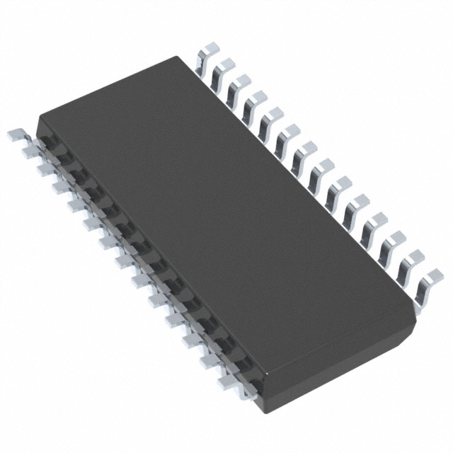
Figure 1. Package
RDS(on)
Iout
VCC
60mΩ (*)
6A (*)
36V
)
s
t(
(*) Per each channel
c
u
d
CMOS COMPATIBLE INPUTS
OPEN DRAIN STATUS OUTPUTS
■ ON STATE OPEN LOAD DETECTION
■ OFF STATE OPEN LOAD DETECTION
■ SHORTED LOAD PROTECTION
■ UNDERVOLTAGE AND OVERVOLTAGE
SHUTDOWN
■ LOSS OF GROUND PROTECTION
■ VERY LOW STAND-BY CURRENT
■
■
REVERSE BATTERY PROTECTION (**)
■ IN COMPLIANCE WITH THE 2002/95/EC
EUROPEAN DIRECTIVE
■
e
t
le
o
s
b
o
r
P
SO-28 (DOUBLE ISLAND)
O
)
s
(
t
c
DESCRIPTION
The VNQ830-E is a quad HSD formed by
assembling two VND830-E chips in the same SO28 package. The VNQ830-E is a monolithic device
made by using| STMicroelectronics VIPower M0-3
Technology. The VNQ830-E is intended for driving
any type of multiple loads with one side connected
to ground. Active V CC pin voltage clamp protects
the device against low energy spikes (see
ISO7637 transient compatibility table).
u
d
o
e
t
e
ol
Pr
Active current limitation combined with thermal
shutdown and automatic restart protects the
device against overload.
The device detects open load condition both in on
and off state. Output shorted to V CC is detected in
the off state. Device automatically turns off in case
of ground pin disconnection.
s
b
O
Table 2. Order Codes
Package
SO-28
Tube
VNQ830-E
Tape and Reel
VNQ830TR-E
Note: (**) See application schematic at page 10
Rev. 2
November 2004
1/21
�VNQ830-E
Figure 2. Block Diagram
VCC1,2
Vcc
OVERVOLTAGE
CLAMP
UNDERVOLTAGE
GND1,2
)
s
t(
CLAMP 1
INPUT1
c
u
d
DRIVER 1
OUTPUT1
o
r
P
CLAMP 2
STATUS1
e
t
le
CURRENT LIMITER 1
DRIVER 2
LOGIC
OVERTEMP. 1
OPENLOAD ON 1
INPUT2
b
O
-
OPENLOAD OFF 1
STATUS2
)
s
(
ct
OVERTEMP. 2
u
d
o
r
P
e
Vcc
CLAMP
t
e
l
o
GND3,4
CURRENT LIMITER 2
OPENLOAD ON 2
OPENLOAD OFF 2
VCC3,4
OVERVOLTAGE
UNDERVOLTAGE
CLAMP 3
bs
OUTPUT3
INPUT3
O
so
OUTPUT2
DRIVER 3
CLAMP 4
STATUS3
CURRENT LIMITER 3
OVERTEMP. 3
LOGIC
DRIVER 4
OUTPUT4
OPENLOAD ON 3
CURRENT LIMITER 4
INPUT4
OPENLOAD OFF 3
OPENLOAD ON 4
STATUS4
OPENLOAD OFF 4
OVERTEMP. 4
2/21
�VNQ830-E
Table 3. Absolute Maximum Ratings
Symbol
VCC
Parameter
Value
Unit
41
V
DC Supply Voltage
- VCC
Reverse DC Supply Voltage
- 0.3
V
- IGND
DC Reverse Ground Pin Current
- 200
mA
Internally Limited
A
-6
A
DC Input Current
+/- 10
mA
DC Status Current
+/- 10
mA
IOUT
- IOUT
IIN
ISTAT
DC Output Current
Reverse DC Output Current
Electrostatic Discharge (Human
R=1.5KΩ; C=100pF)
VESD
Body
4000
- INPUT
od
5000
r
P
e
5000
- VCC
Maximum Switching Energy
Ptot
(L=2.5mH; RL=0Ω; Vbat=13.5V; Tjstart=150ºC;
IL=9A)
Tstg
Storage Temperature
)
(s
let
so
Power dissipation (per island) at Tlead=25°C
Junction Operating Temperature
Tj
uc
4000
- STATUS
- OUTPUT
EMAX
)
s
t(
Model:
Ob
V
V
V
V
140
mJ
6.25
W
Internally Limited
°C
- 55 to 150
°C
Figure 3. Configuration Diagram (Top View) & Suggested Connections for Unused and N.C. Pins
t
c
u
od
VCC1,2
Ob
so
e
t
e
l
Pr
1
28
VCC1,2
GND 1,2
OUTPUT1
INPUT1
OUTPUT1
STATUS1
OUTPUT1
STATUS2
OUTPUT2
INPUT2
OUTPUT2
VCC1,2
OUTPUT2
VCC3,4
OUTPUT3
GND 3,4
OUTPUT3
INPUT3
OUTPUT3
STATUS3
OUTPUT4
STATUS4
OUTPUT4
INPUT4
OUTPUT4
VCC3,4
Connection / Pin Status
Floating
X
To Ground
14
N.C.
X
X
15
Output
X
VCC3,4
Input
X
Through 10KΩ resistor
3/21
�VNQ830-E
Figure 4. Current and Voltage Conventions
IS3,4
IS1,2
VCC3,4
VCC3,4
VCC1,2
VF1 (*)
VCC1,2
IIN1
INPUT1
ISTAT1
VIN1
IIN2
VSTAT1
OUTPUT3
IOUT4
INPUT4
VIN4 ISTAT4
OUTPUT4
STATUS4
GND3,4
VSTAT4
e
t
le
o
r
P
O
)
s
(
t
c
Parameter
u
d
o
Rthj-lead
Thermal Resistance Junction-lead per chip
Rthj-amb
Thermal Resistance Junction-ambient (one chip ON)
Rthj-amb
IGND1,2
Pr
Thermal Resistance Junction-ambient (two chips ON)
e
t
e
ol
c
u
d
VOUT3
o
s
b
(*) VFn = VCCn - VOUTn during reverse battery condition
Symbol
VOUT4
GND1,2
IGND3,4
Table 4. Thermal Data (Per island)
)
s
t(
VOUT2
IOUT3
STATUS3
IIN4
VSTAT3
OUTPUT2
INPUT3
ISTAT3
VIN3
VOUT1
IOUT2
STATUS2
IIN3
VSTAT2
OUTPUT1
INPUT2
ISTAT2
VIN2
IOUT1
STATUS1
60 (1)
1
46 ( )
Value
Unit
20
°C/W
44 (2)
°C/W
31 (2)
°C/W
Note: 1. When mounted on a standard single-sided FR-4 board with 0.5cm 2 of Cu (at least 35µm thick) connected to all V CC pins. Horizontal
mounting and no artificial air flow
Note: 2. When mounted on a standard single-sided FR-4 board with 6cm 2 of Cu (at least 35µm thick) connected to all VCC pins. Horizontal
mounting and no artificial air flow
s
b
O
4/21
�VNQ830-E
ELECTRICAL CHARACTERISTICS
(8V VOL
O
)
u
d
o
VSTATn
e
t
e
ol
Pr
tDOL(off)
H
L
OVER TEMP STATUS TIMING
IOUT < IOL
s
(
t
c
VINn
o
s
b
o
r
P
L
H
Tj > TTSD
VINn
VSTATn
tSDL
tSDL
tDOL(on)
s
b
O
7/21
�VNQ830-E
Figure 6. Switching time Waveforms
VOUTn
90%
80%
dVOUT/dt(off)
dVOUT/dt(on)
)
s
t(
10%
t
VINn
td(on)
td(off)
e
t
le
c
u
d
o
r
P
so
)
s
(
ct
b
O
-
t
Table 13. Electrical Transient Requirements On V CC Pin
ISO T/R 7637/1
Test Pulse
1
2
3a
3b
4
5
e
t
e
ol
s
b
O
ISO T/R 7637/1
Test Pulse
1
2
3a
3b
4
5
CLASS
C
E
8/21
du
I
o
r
P
-25 V
+25 V
-25 V
+25 V
-4 V
+26.5 V
I
C
C
C
C
C
C
II
TEST LEVELS
III
IV
-50 V
+50 V
-50 V
+50 V
-5 V
+46.5 V
-75 V
+75 V
-100 V
+75 V
-6 V
+66.5 V
-100 V
+100 V
-150 V
+100 V
-7 V
+86.5 V
TEST LEVELS RESULTS
II
III
C
C
C
C
C
C
C
C
C
C
E
E
Delays and
Impedance
2 ms 10 Ω
0.2 ms 10 Ω
0.1 µs 50 Ω
0.1 µs 50 Ω
100 ms, 0.01 Ω
400 ms, 2 Ω
IV
C
C
C
C
C
E
CONTENTS
All functions of the device are performed as designed after exposure to disturbance.
One or more functions of the device is not performed as designed after exposure and cannot be
returned to proper operation without replacing the device.
�VNQ830-E
Figure 7. Waveforms
NORMAL OPERATION
INPUTn
LOAD VOLTAGEn
STATUSn
)
s
t(
UNDERVOLTAGE
VUSDhyst
VCC
c
u
d
VUSD
INPUTn
LOAD VOLTAGEn
STATUS
undefined
e
t
le
OVERVOLTAGE
o
s
b
VCCVOV
VCC
O
)
INPUTn
LOAD VOLTAGEn
STATUSn
INPUTn
s
(
t
c
u
d
o
Pr
LOAD VOLTAGEn
STATUSn
e
t
e
ol
O
bs
o
r
P
OPEN LOAD with external pull-up
VOUT>VOL
VOL
OPEN LOAD without external pull-up
INPUTn
LOAD VOLTAGEn
STATUSn
Tj
TTSD
TR
OVERTEMPERATURE
INPUTn
LOAD CURRENTn
STATUSn
9/21
�VNQ830-E
Figure 8. Application Schematic
+5V +5V
+5V
VCC1,2
VCC3,4
Rprot
STATUS1
Rprot
INPUT1
)
s
(
Dld
Rprot
STATUS2
Rprot
INPUT2
µC
Rprot
INPUT3
Rprot
)
s
(
ct
STATUS4
Rprot
du
e
t
e
ol
d
o
r
P
e
et
l
o
s
STATUS3
Rprot
t
c
u
OUTPUT1
b
O
-
OUTPUT2
OUTPUT3
OUTPUT4
INPUT4
o
r
P
GND1,2
GND3,4
RGND
VGND
+5V +5V
DGND
s
b
O
Note: Channels 3 & 4 have the same internal circuit as channel 1 & 2.
GND PROTECTION
REVERSE BATTERY
NETWORK
AGAINST
Solution 1: Resistor in the ground line (RGND only). This
can be used with any type of load.
The following is an indication on how to dimension the
RGND resistor.
1) RGND ≤ 600mV / 2(IS(on)max).
2) RGND ≥ (−VCC) / (-IGND)
where -IGND is the DC reverse ground pin current and can
be found in the absolute maximum rating section of the
device’s datasheet.
Power Dissipation in RGND (when VCC
很抱歉,暂时无法提供与“VNQ830TR-E”相匹配的价格&库存,您可以联系我们找货
免费人工找货