UM1955
User manual
Getting started with the multifunctional expansion board based on
operational amplifiers for STM32 Nucleo
Introduction
The X-NUCLEO-IKA01A1 is a multifunctional expansion board based on operational
amplifiers. It provides an easy-to-use and affordable solution for different multifunctional use
cases with your STM32 Nucleo board. The X-NUCLEO-IKA01A1 is compatible with the
Arduino™ UNO R3 connector, and supports the addition of other boards that can be
stacked for enhanced applications with an STM32 Nucleo expansion board. It can be used
as a analog front-end by conditioning signals as an actuator to drive LED or coils, or in a
comparator architecture. Thanks to its current-sensing configuration, it allows current
measurement of any device that has a USB port. For this configuration and the
instrumentation amplifier configuration, a highly accurate operational amplifier (TSZ124) is
used. The expansion board also contains Nanopower (TSU104) and Micropower (TSV734)
operational amplifiers for mobile applications.
This user manual describes how to use the predefined configurations of the X-NUCLEOIKA01A1 expansion board:
•
Instrumentation amplifier structure
•
Current sensing with or without USB port
•
Photodiode/UV current sensing
•
Buffer
•
Full wave rectifier
•
Constant current LED driver
•
Window comparator
The expansion board is also equipped with one prototyping area is powered through the
Arduino UNO R3 connectors.
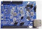
Figure 1. X-NUCLEO-IKA01A1 multifunctional expansion board
October 2015
DocID028405 Rev 1
1/28
www.st.com
28
�Contents
UM1955
Contents
1
2
3
4
5
6
7
2/28
Instrumentation amplifier configuration . . . . . . . . . . . . . . . . . . . . . . . . . 4
1.1
Schematic diagram . . . . . . . . . . . . . . . . . . . . . . . . . . . . . . . . . . . . . . . . . . . 4
1.2
How to set up the board . . . . . . . . . . . . . . . . . . . . . . . . . . . . . . . . . . . . . . . 4
1.3
Theoretical output . . . . . . . . . . . . . . . . . . . . . . . . . . . . . . . . . . . . . . . . . . . . 5
1.4
Software and measurements . . . . . . . . . . . . . . . . . . . . . . . . . . . . . . . . . . . 5
Current sensing configuration . . . . . . . . . . . . . . . . . . . . . . . . . . . . . . . . . 6
2.1
Schematic diagram . . . . . . . . . . . . . . . . . . . . . . . . . . . . . . . . . . . . . . . . . . . 6
2.2
How to set up the board . . . . . . . . . . . . . . . . . . . . . . . . . . . . . . . . . . . . . . . 7
2.3
Theoretical output . . . . . . . . . . . . . . . . . . . . . . . . . . . . . . . . . . . . . . . . . . . . 7
2.4
Software and measurements . . . . . . . . . . . . . . . . . . . . . . . . . . . . . . . . . . . 8
Buffer configuration . . . . . . . . . . . . . . . . . . . . . . . . . . . . . . . . . . . . . . . . . 9
3.1
How to set up the board . . . . . . . . . . . . . . . . . . . . . . . . . . . . . . . . . . . . . . . 9
3.2
Theoretical output . . . . . . . . . . . . . . . . . . . . . . . . . . . . . . . . . . . . . . . . . . . . 9
Full wave rectifier . . . . . . . . . . . . . . . . . . . . . . . . . . . . . . . . . . . . . . . . . . 10
4.1
Schematic diagram . . . . . . . . . . . . . . . . . . . . . . . . . . . . . . . . . . . . . . . . . . 10
4.2
How to set up the board . . . . . . . . . . . . . . . . . . . . . . . . . . . . . . . . . . . . . . 10
4.3
Theoretical output . . . . . . . . . . . . . . . . . . . . . . . . . . . . . . . . . . . . . . . . . . . 10
4.4
Measurement example . . . . . . . . . . . . . . . . . . . . . . . . . . . . . . . . . . . . . . . 10
Photodiode/UV sensor . . . . . . . . . . . . . . . . . . . . . . . . . . . . . . . . . . . . . . 11
5.1
Schematic diagram . . . . . . . . . . . . . . . . . . . . . . . . . . . . . . . . . . . . . . . . . . .11
5.2
How to set up the expansion board . . . . . . . . . . . . . . . . . . . . . . . . . . . . . .11
5.3
Measurement example . . . . . . . . . . . . . . . . . . . . . . . . . . . . . . . . . . . . . . . .11
5.4
Additional possible use . . . . . . . . . . . . . . . . . . . . . . . . . . . . . . . . . . . . . . . 12
LED driver configuration . . . . . . . . . . . . . . . . . . . . . . . . . . . . . . . . . . . . 13
6.1
Schematic diagram . . . . . . . . . . . . . . . . . . . . . . . . . . . . . . . . . . . . . . . . . . 13
6.2
How to set up the board . . . . . . . . . . . . . . . . . . . . . . . . . . . . . . . . . . . . . . 14
Window comparator configuration . . . . . . . . . . . . . . . . . . . . . . . . . . . . 15
DocID028405 Rev 1
�UM1955
Contents
7.1
Schematic diagram . . . . . . . . . . . . . . . . . . . . . . . . . . . . . . . . . . . . . . . . . . 15
7.2
How to set up the board . . . . . . . . . . . . . . . . . . . . . . . . . . . . . . . . . . . . . . 15
7.3
Theoretical output . . . . . . . . . . . . . . . . . . . . . . . . . . . . . . . . . . . . . . . . . . . 16
8
Prototyping area . . . . . . . . . . . . . . . . . . . . . . . . . . . . . . . . . . . . . . . . . . . 17
9
Scenario examples . . . . . . . . . . . . . . . . . . . . . . . . . . . . . . . . . . . . . . . . . 18
9.1
Current sensing: motor outside of standard operation . . . . . . . . . . . . . . . 18
9.2
Strain gauge . . . . . . . . . . . . . . . . . . . . . . . . . . . . . . . . . . . . . . . . . . . . . . . 18
9.3
Electromyogram . . . . . . . . . . . . . . . . . . . . . . . . . . . . . . . . . . . . . . . . . . . . 18
9.4
Body detection . . . . . . . . . . . . . . . . . . . . . . . . . . . . . . . . . . . . . . . . . . . . . 19
10
Operational amplifiers on the expansion board . . . . . . . . . . . . . . . . . . 20
11
Schematic diagrams . . . . . . . . . . . . . . . . . . . . . . . . . . . . . . . . . . . . . . . . 21
12
Bill of material (BOM) . . . . . . . . . . . . . . . . . . . . . . . . . . . . . . . . . . . . . . . 23
13
Revision history . . . . . . . . . . . . . . . . . . . . . . . . . . . . . . . . . . . . . . . . . . . 27
DocID028405 Rev 1
3/28
28
�Instrumentation amplifier configuration
1
UM1955
Instrumentation amplifier configuration
The instrumentation amplifier configuration allows you to amplify a differential signal without
impacting it thanks to the high impedance of operational amplifier input stage. Moreover,
with the high accuracy resistors, this configuration features high rejection to common mode
voltage.
1.1
Schematic diagram
Figure 2 below depicts the circuit schematic of the instrumentation amplifier configuration.
Figure 2. Instrumentation amplifier configuration circuit schematic
9UHI
*1'
�
�
-3�
5�
&�
��Q)
�
5�
�0
1&
�9
&�
�
,QVWBQ
9�
��S)
�
��
�
�
9�
76=���,37� �$
5�
�
��N
*1'
-3�
��N
5�
5JDLQBD
5�
��N
(6'�
�
*1'
,�2�
�
*1'
�
,�2�
,�2�
9EXV
,�2�
�
�
�
-3�
�9
�
��
76=���,37� �&
5JDLQBE
73�
5��
��N
&��
�
5J
�N
(6'$/&/���6&�
73�
�
�
$�
���S)
5��
��N
*1'
�
�
�
�
&�
�
��S)
5�
�0
1&
,QVWBS
9UHI
*1'
5�
��N
-3�
5�
��N
9UHI
5�� 76=���,37� �%
�
�
�9
-3�
1.2
5�
��N
*63*��������',����
How to set up the board
The instrumentation amplifier section of the expansion board includes several jumpers for
improved versatility. For this configuration, jumpers JP2, JP4 and JP5 must be mounted and
JP6 and JP7 should not be mounted. If the input signal is capacitive, a bias voltage needs to
be added. This configuration is possible by mounting jumpers JP6 and JP7. Once jumpers
have been set in the required configuration, the differential must be connected to pins Inst_n
and Inst_p.
4/28
DocID028405 Rev 1
�UM1955
1.3
Instrumentation amplifier configuration
Theoretical output
The theoretical output voltage is defined by the following formula:
Equation 1
The operational amplifiers used for this configuration are used with a 5 V power supply.
Thus in order to obtain a range limited to 3.3 V to avoid any damage on the microcontroller
side, a divider bridge has been implemented. This additional structure is recognizable by the
last term in the above formula (composed of R37 and R38). Thanks to this structure, a DC 5
V output voltage is reduced to 3.2 V.
The gain of this instrumentation amplifier structure is defined by:
Equation 2
Note that it is also possible to increase the gain of the configuration by adding an external
resistor on the Rgain_a and Rgain_b pins. When an external resistor is used to change the
gain, jumper JP2 must be unmounted.
With this circuitry, the maximum frequency of the input signal is 850 Hz based on the opamp GBP and the circuit gain.
Equation 3
The factor 10 is taken in order to take margin and to properly amplify the signals at the
maximum frequency.
1.4
Software and measurements
The output voltage of the instrumentation amplifier is connected to the pin A1 of the Arduino
UNO R3 connector. The X-CUBE-ANALOG1 software available on www.st.com allows
users to measure this voltage.
DocID028405 Rev 1
5/28
28
�Current sensing configuration
2
UM1955
Current sensing configuration
The current sensing configuration allows monitoring of the current that is consumed by an
application. On this expansion board, the operational amplifier is set to a high-side current
sensing structure. This means that the current is measured close to the supply voltage, thus
before the application. Figure 3 illustrates this concept.
Figure 3. High-side current sensing application principle
2.1
Schematic diagram
Figure 4, shows the circuit schematic of the current sensing configuration.
Figure 4. Current sensing configuration circuit schematic
*1'
-�
'XVE
0LFUR� 86%
9EXV
'� �
'�
,'
*1'
5��
�0
�
�
�
�
�
�
&I�
���Q)
5J�
���
,LQ
&��
��Q)
*1'
'�
'� �
9EXV
�
�
�
5V
��P
�
,RXW
�
-�
5I�
��N
��
��
5J�
���
76=���,37� �'
5��
��
��N
&��
5I�
��N
&I�
���S)
$�
5��
��N
*1'
*1'
���Q)
86%� $
*63*��������',����
6/28
DocID028405 Rev 1
�UM1955
2.2
Current sensing configuration
How to set up the board
With this expansion board, users can measure the current of a USB-powered device or any
5 V application. It is important not to go beyond 5 V in order to avoid operational amplifier
damage. To help protect the circuit, an ESDAULC6-1U2 unidirectional ESD protection
device has been implemented.
Monitoring USB-powered device current: connect the charger (wall adapter or PC) to the
Micro-USB port. Then connect the bottom USB port to the required device.
Monitoring other application current: it is also possible to measure the current of
applications that are not USB powered. The power supply voltage should be connected to
Iin, and Iout should be connected to the power supply voltage pin of the application.
2.3
Theoretical output
The output voltage of the operational amplifier is proportional to the measured current, as
the following formula illustrates:
Equation 4
Therefore,
Equation 5
Similar to the instrumentation amplifier configuration, the operational amplifier for this
configuration is used with a 5 V power supply voltage. Thus, in order to obtain a range
limited to 3.3 V avoid damage on the microcontroller side, a divider bridge has been added.
This additional structure is recognizable by the last term in the above formula (composed by
R30 and R39). Thanks to this structure, a DC 5 V output voltage is reduced to a 3.2 V.
Note that the maximum frequency of this circuit is limited to 330 Hz based on operational
amplifier GBP and the circuit gain.
Equation 6
DocID028405 Rev 1
7/28
28
�Current sensing configuration
2.4
UM1955
Software and measurements
The output voltage of the instrumentation amplifier is connected to pin A2 of the Arduino
UNO R3 connector. The X-CUBE-ANALOG1 software, available on www.st.com, allows
users to measure this voltage.
Note that with this predefined configuration, it is possible to measure up to 2.08 A. If a
higher current is drawn through the application, the operational amplifier will be saturated
and thus its output voltage will not reflect the real current.
The following table shows the correspondence between measured current, output voltage
and LSB on ADC.
Table 1. Output parameter values for current sensing configuration
8/28
Current (A)
Output voltage of
operational amplifier
Voltage after divider
bridge (at A4 node)
Number of LSBs with
12-bit ADC
0.1
240 mV
159 mV
197
0.2
480 mV
317 mV
394
0.5
1.20 V
793 mV
985
1.0
2.40 V
1.586 V
1969
1.5
3.60 V
2.380 V
2954
2.0
4.80 V
3.173 V
3938
DocID028405 Rev 1
�UM1955
3
Buffer configuration
Buffer configuration
The buffer configuration allows users to connect a high output impedance circuit to a low
input impedance circuit without disturbing the signal. This function is possible thanks to the
high impedance of the operational amplifier input stage and the operational amplifier output
capabilities. The operational amplifier used for this configuration is the TSV734, which has a
minimum output current of 40 mA.
3.1
How to set up the board
In order to use the buffer configuration on the expansion board, users simply connect their
signal to the “in” pin on the buffer section of the board. The output signal can be retrieved on
the “out” pin in the same board section. The output voltage of the operational amplifier is not
intended to be connected to any microcontroller input on the expansion board since this
configuration is most often used before another circuit.
3.2
Theoretical output
The output voltage of the operational amplifier is equal to its input voltage:
Vout=Vin
Note that this equation is correct as long as the input voltage stays between 0 V and 3.3 V
(the power supply voltage of the operational amplifier).
DocID028405 Rev 1
9/28
28
�Full wave rectifier
4
UM1955
Full wave rectifier
The full wave rectifier configuration allows rectification of an input signal. This means that by
defining a reference voltage with a potentiometer, all signals below it will become positive.
When the voltage goes above the reference, the output voltage will not change.
4.1
Schematic diagram
Figure 5 shows the circuit schematic of the full wave rectifier configuration.
Figure 5. Full wave rectifier configuration circuit schematic
��N
��N
��N
$
5��
�
9&&
�
'�
5HFWBRXW
�
�
&�
*1'
'�
5��
��N
769���,37��%
���)
*1'
��
$
3�
���N
�
.
��N
5��
.
5HFWBLQ 5��
5��
&��
���S)
769���,37��&
*1'
5��
��N
*63*��������',����
4.2
How to set up the board
The input signal must be connected to the Rect_in pin within the rectifier expansion board
section. Similarly, the output signal is available on the Rect_out pin. The output voltage of
the rectifier structure is not intended to be connected to any microcontroller input on the
board since this configuration is most often connected to another analog block.
4.3
Theoretical output
Thus, we have two formulas to define this configuration:
If Vin < Vref: Vout = 2Vref - Vin
If Vin ≥ Vref: Vout = Vin
The Vref voltage can be tuned using the P1 potentiometer.
4.4
Measurement example
Input voltage = -1 V
Vref = 0.5 V
Thus, Vout = 2 V
10/28
DocID028405 Rev 1
�UM1955
5
Photodiode/UV sensor
Photodiode/UV sensor
This configuration can be used to monitor the ambient light and, for example, trigger an
action when a threshold level is reached.
5.1
Schematic diagram
Figure 6 depicts the circuit schematic of photodiode sensor configuration.
Figure 6. Photodiode configuration circuit schematic
&��
���S)
���N
5��
��
��
��
89
1&
768���,37� �'
'�
*1'
5��
��N
$�
&��
���S)
*1'
*1'
*63*��������',����
5.2
How to set up the expansion board
This configuration does not require any setup. Only the output voltage is reported. This
voltage is available on pin A4 of the Arduino UNO R3 connector and PC1 of the ST morpho
connectors (not mounted in the expansion board).
5.3
Measurement example
Here, three examples have been selected.
•
Case 1: The board is placed inside a closed box. Vout = 33 mV (Vol of the operational
amplifier which is saturating)
•
Case 2: The board is in ambient light Vout = 420 mV
•
Case 3: The sensor is below a light source Vout = 3.272 V (Voh of the operational
amplifier which is saturating)
Depending on the needs of the application, it can be interesting to have current with better
sensitivity to darkness. In this case, it is recommended to increase the value of the R26
DocID028405 Rev 1
11/28
28
�Photodiode/UV sensor
UM1955
resistor. When current is flowing through a resistor which has a large value, it is mandatory
to use an operational amplifier with a very low input current offset. This is why operational
amplifiers with a CMOS input stage, such as the TSU104, are required.
5.4
Additional possible use
With this configuration it is also possible to connect a UV (ultraviolet) sensor in order to
derive the UV index instead of ambient light. A free footprint is available on the expansion
board to enable this possibility.
Note that if using a UV sensor, R26 should be aligned to the UV sensor datasheet
recommendation and the photodiode must be removed.
For additional details on the analog conditioning circuit used for a high impedance sensor
and especially on a UV sensor, refer to application note AN4451 “Signal conditioning for a
UV sensor”, available on www.st.com.
12/28
DocID028405 Rev 1
�UM1955
6
LED driver configuration
LED driver configuration
The LED driver configuration allows users to drive an LED with a constant current. As
shown in Figure 7, when the forward voltage varies, the current and thus the light intensity is
highly variable.
Figure 7. Forward current vs. forward voltage
This is why it is recommended to control the LED by current, and thus this architecture is
useful.
Schematic diagram
Figure 8 shows the circuit schematic of the LED driver configuration.
Figure 8. LED driver configuration circuit schematic
9DQD
'�
/('B$
�
/('B.
�
�
-3�
��Q)
769���,37��'
5��
�N
��
��
�
&
��
&��
%
4�
131
�
���N
5��
5��
�0
(
'�
*1'
*1'
&��
��S)
&��
1&
*1'
DocID028405 Rev 1
5��
�N
��
6.1
5��
*1'
*63*��������',����
13/28
28
�LED driver configuration
6.2
UM1955
How to set up the board
There is no specific connection to make the application function, but a PWM input signal is
required on pin D3 of the Arduino UNO R3 connector.
One or several external LEDs in parallel can be added in order to drive several LEDs at the
same time. LEDs can be connected to pin LED_A and LED_K on the expansion board.
Moreover, if needed it is possible to disconnect the mounted LED by removing jumper JP1.
Note also that the supply voltage of the LED can be either external or based on the internal
3.3 V. If several LEDs are in parallel or a higher power is needed, it is recommended to
place the Vcc jumper in the Vext position and use an external power supply.
Depending the PWM duty cycle, the LED intensity will vary. For a duty cycle of 5% (5% of
the time at high state), the intensity will be low. On the other hand, for a 70% duty cycle, the
light intensity will be high.
14/28
DocID028405 Rev 1
�UM1955
7
Window comparator configuration
Window comparator configuration
The window comparator configuration allows the user to compare a signal to two threshold
voltages. When the signal is out of the required voltage range, the output of the operational
amplifier toggles.
7.1
Schematic diagram
Figure 9 shows the schematic of the window comparator configuration.
Figure 9. Window comparator configuration circuit schematic
9FF
5��
��N
9FF
&��
�
9�
'�
'�
*1'
3�
���N
�
�
:LQBLQ
�
5��
��N
(6'�
768���,37� �$
9�
�
��
5��
��N
�
��Q)
�
768���,37� �%
(6'$/&�9���0�
*1'
*1'
7.2
*63*��������',����
How to set up the board
To set up the expansion board, connect the signal to the “in” pin within the window
comparator section. The high and low threshold voltages then need to be defined by tuning
the P2 potentiometer.
Threshold voltages:
Equation 7
DocID028405 Rev 1
15/28
28
�Window comparator configuration
UM1955
Equation 8
•
•
If P2 equals its maximum value (500 k):
–
Vth_low = 62 mV
–
Vth_high = 3.238 V
If P2 equals its minimum value (0):
–
Vth_low = 1.1 V
–
Vth_high = 2.2 V
From a software standpoint, the D2 and D4 pins on the Arduino UNO R3 connectors or
PA10 and PB5 on the ST morpho connectors (not mounted in the expansion board) must be
monitored.
7.3
Theoretical output
The operational amplifier output toggles when the signal is out of the specified window.
Vin < Vthreshold_low:
D2: high state
D4: low state
Vthreshold_low < Vin < Vthreshold_high:
D2: high state
D4:high state
Vthreshold_high < Vin:
D2: low state
D4: high state
Figure 10 depicts the different states:
Figure 10. Window comparator explanation
16/28
DocID028405 Rev 1
�UM1955
8
Prototyping area
Prototyping area
A prototyping area has been implemented in order to perform small additional
configurations.
It allows the user to connect an expansion board, components on input and output, and a
divider bridge for a 5 V to 3.3 V conversion, as shown on the following figure.
Figure 11. Prototyping area
Note also that the supply voltage of the operational amplifier can be either external or based
on the internal 3.3 V. If a high output voltage and thus a higher power supply voltage is
required, it is recommended to place jumper JP3 in the Vext position.
DocID028405 Rev 1
17/28
28
�Scenario examples
UM1955
9
Scenario examples
9.1
Current sensing: motor outside of standard operation
To avoid damage to an application, it can be useful to know how much current is going
through the motor. With the high-side current sensing or instrumentation amplifier
configuration, the current can be monitored. The motor can be in different configurations:
stopped, in standard operating condition or in overload. By sensing the current, it is easy to
detect the configuration of the motor. Thus we can set some flag to alert the user or the
microcontroller. If the current is too low or too high, the output of the window comparator will
toggle. Then, for example, when the motor is in a standard operating range, the LED can
illuminate with a low intensity, but if the current is out of range, the LED can blink with a high
intensity. The threshold current can be adjusted thanks to potentiometer P2 with the window
comparator configuration. Of course, an LED is used here as an example in order to obtain
a visual response, but it can also be useful to capture the interruption at the output of the
window comparator. By doing this, it would be possible to stop the motor or to perform
another action in order to prevent damage to the application.
This scenario uses the following configuration available on the expansion board:
•
Current sensing or instrumentation amplifier structure
•
Window comparator
•
LED driver
Note that with the instrumentation amplifier configuration, an external shunt resistor is
required. But it will allow you to sense the current in both clockwise and counter-clockwise
directions.
9.2
Strain gauge
Having some strain gauge composing a Wheatstone bridge, the instrumentation amplifier
can help you to detect deformation. These deformations can be, for example, for structure
monitoring, for torque monitoring or even to develop your own scale for weight
measurement.
9.3
Electromyogram
An electromyogram (EMG) application can help users monitor muscle electrical activity. It
can be used to trigger an action by contracting your arm, for example.
The signal generated by the muscle is a very small AC signal. This is why it is mandatory to
amplify it. Then its envelop must be detected. Envelop detection should be performed with
an accurate rectifier in order to avoid losing diode voltage. Thus is why an active
configuration with operational amplifiers is used. Once the signal is rectified, we just need to
filter the signal. It can be done on the microcontroller side, by software or with its integrated
operational amplifier. Figure 12 shows the signal conditioning for an EMG application.
18/28
DocID028405 Rev 1
�UM1955
Scenario examples
Figure 12. Electromyogram signal conditioning
2.0
After amplification
After rectifier
After filter with gain
1.8
Voltages (V)
1.5
1.3
1.0
0.8
0.5
0.3
0.0
0
1
2
3
4
5
Time (s)
This scenario uses the following configuration available on the expansion board:
9.4
•
Instrumentation amplifier structure
•
Full wave rectifier
•
Window comparator to perform an action depending on muscle activity level
Body detection
With the use of an external passive infrared (PIR) sensor, it is possible to light a room with
the different configurations available on the expansion board. The signal generated by the
PIR sensor will be amplified. Then this analog signal can be converted to a digital signal
thanks to the window comparator. When the sensor detects motion, based on an emissivity
difference the output of the comparator will toggle. The comparator output can be coupled to
the photodiode sensor which indicates whether it is day or night. This functionality allows
lighting a room only at night.
Note that the LED driver configuration contains a slot for plugging in additional LEDs in
parallel if. for example, you wish to provide light in several directions at the same time.
This scenario uses the following configuration available on the expansion board:
•
Instrumentation amplifier structure (used in standard gain configuration)
•
Photodiode sensor
•
Window comparator
•
LED driver
High-pass and low-pass filtering can be performed by software or with microcontrollerintegrated operational amplifiers or even with external components on the expansion board
prototyping area.
For more details on PIR signal conditioning, please refer to application note AN4368 “Signal
conditioning for pyroelectric passive infrared (PIR) sensors”, available on www.st.com
DocID028405 Rev 1
19/28
28
�Operational amplifiers on the expansion board
10
UM1955
Operational amplifiers on the expansion board
Table 2 summarizes the main parameters of the operational amplifiers used on this analog
expansion board.
Table 2. Operational amplifier main parameters
Configuration on
the expansion
board
Note:
20/28
Icc per
amplifier
(µA)
GBP
(kHz)
Vio max
(µV)
Comments
TSZ124
Instrumentation
amplifier, current
sensing
31
400
5
5 V operational amplifier
Very high accuracy
Available in QFN package
TSV734
Buffer, rectifier, LED
driver
59
850
200
5 V operational amplifier
High accuracy
Available in QFN package
TSU104
Photodiode
structure, window
comparator
0.6
8
3000
5 V operational amplifier
Nanopower
Available in QFN package
Current consumption is mentioned per amplifier. The TSZ124, TSV734 and TSU104 contain
four operational amplifiers in the same package.
DocID028405 Rev 1
�5��
�5
$�
*1'
1&
&��
*1'
��Q)
��
�
��
��
��
��
��
�
�
�
�
�
�
�
�
$�
$�
$�
$�
$�
$�
,25HI
5HVHW
���9
�9
*1'
*1'
9LQ
',*,7$/� �3:0� a�
��S)
&��
5��
�N
769���,37� �'
5��
��
�N
/('B.
/('B$
/('� GULYHU
&1�
��
*1'
&��
*1'
5��
�5
$�
*1'
5��
�5
���N
5��
5��
�0
'�
&�
���)
�9
$�
*1'
���)
&�
9&&
&1�
32:(5
$1$/2*� ,1
��
��
��
��
��
��
��
��
�
%
-3�
�
a�
a�
�
a�
�
7;� �
5;� �
$UHI
*1'
��
��
a��
a��
a�
�
��
��
��
��
��
��
��
��
��
��
�
�
&1�
&1�
*1'
5��
4�
131
'�
9DQD
*1'
9FF
5��
'�
�5
5��
'�
�5
5��
'�
�5
,Q�%
3U��
,Q�$
,Q�$
,Q�%
9H[W
9H[W �
3U��
3U��
3U�
9DQD �
�
-3�
*1'
���)
&��
�
��
9�
9�
*1'
2S$PS%
3U� 3U� 3U� 3U�
3U� 3U� 3U� 3U�
�
�
�
�
*1'
�
�
2XW%
2XW$
2S$PS$
��Q)
&��
9DQD
5��
*1'
5��
��N
2XW$�
9UHI
*1'
2XW%�
2XW %�
5��
��N
5��
��N
5��
��N
2XW$�
���N
*1'*1'
���S)
&��
768���,37� �&
�
3URWR�W\SLQJ� DUHD
*1'
5��
��N
5��
��N
9&&
,QWHUQDO� EXIIHU
�
$UGXLQRB8QR
$UGXLQR� 812
�
&
(
�
��
DocID028405 Rev 1
�
3U��
3U��
3U��
3U��
*1'
(6'$/&�9���0�
(6'�
3�
���N
89
1&
:LQBLQ
5��
��N
5��
��N
9FF
9�
9�
$QG� JDWH
*1'
'�
*1'
��
��
��
768���,37� �'
���N
5��
���S)
&��
5��
��N
*1'
���S)
&��
$�
'� ,I�RXWSXW�ORZ��RXW�RI�ZLQGRZ
'�
768���,37� �%
�
*1'
768���,37� �$
�
��Q)
3KRWRGLRGH� �� 89� VHQVRU
*1'
5��
��N
�
�
�
�
9FF
&��
:LQGRZ���������������������
� &RPSDUDWRU
�
�
��
11
$UGXLQR��812�5��&RQQHFWRUV
UM1955
Schematic diagrams
Schematic diagrams
Figure 13. X-NUCLEO-IKA01A1 circuit schematic (1 of 2)
*63*��������',����
21/28
28
�,�2�
*1'
,�2�
,�2�
9EXV
,�2�
-3�
��S)
&�
�
�
�
9UHI
,QVWBS
-3�
%XIIBLQ
��S)
�9
5�
�0
5JDLQBE
�
&�
-3�
�
5�
�0
5JDLQBD
(6'$/&/���6&�
�
�
�
�
*1'
�
�
(6'�
,QVWBQ
�
�
�
1&
�9
�
�
9�
9�
5�
��N
-3�
��N
5�
*1'
�
�
�
769���,37� �$ ��Q)
9FF
&��
%XIIHU
5�
��N
76=���,37� �$
5�
�
��N
��Q)
�9
&�
5�� 76=���,37� �%
5J
�N
�
�
�
�
5�
*1'
�
��
9UHI
9�
9�
�
*1'
��
1&
�
�
,�2�
*1'
,�2�
,�2�
9EXV
,�2�
�
�
�
9UHI
73�
5��
9FF
*1'
���S)
5��
��N
&��
%XIIBRXW
(6'$/&/���6&�
�
�
�
(6'�
5�
��N
76=���,37� �&
5�
��N
*1'*1'
���S)
&�
��
�
,QVWUXPHQWDWLRQ� DPSOLILHU
���N
*1'
$�
5HFWBLQ
5��
��N
73�
&�� ��Q)
5��
�0
��N
5��
-�
-�
86%� $
�
�
�
�
�
�
�
�
�
�
�
*1'
���N
3�
9&&
9EXV
*1'
'�
'� �
9EXV
'� �
'�
,'
*1'
0L FUR� 86%
*1'
*1'
��N
5��
�
��N
5��
769���,37� �%
���)
&�
�
�
5V
&I�
5J�
���
5J�
���
���Q)
'�
'�
�
769���,37� �&
��N
��
5��
���Q)
&I�
��N
5��
*1'
���S)
&��
*1'
���S)
76=���,37� �'
5��
��
��N
&��
5I�
��N
��N
�
��
��
5I�
��N
5��
)XOO� ZDYH� 5HFWLILHU
,RXW
,LQ
'XVE
+LJK� VLGH� FXUUHQW� VHQVLQJ � FRQILJXUDWLRQ
��P
$
.
DocID028405 Rev 1
$
22/28
.
-3�
$�
5HFWBRXW
*1'
5��
��N
Schematic diagrams
UM1955
Figure 14. X-NUCLEO-IKA01A1 circuit schematic (2 of 2)
*63*��������',����
�UM1955
Bill of material (BOM)
12
Bill of material (BOM)
Table 3. Bill of material (part 1)
Voltage
Watt
Ampere
Item
Qty
Ref.
Part / value
1
4
C0, C1, C7, C14
0.1 µF
SMD0603
2
5
C2, C12, C17, C18, C23
22 nF
SMD0603
3
2
C3, C4
22 pF
SMD0603
4
7
C9, C15, C16, C19, C20,
C21, C22
100 pF
SMD0603
5
1
C10
47 pF
SMD0603
6
1
C11
Not mounted
SMD0603
7
2
R8, R10
Not mounted
SMD0603
8
1
UV
Not mounted
SMD0805
9
1
C13
47 nF
SMD0603
10
2
Cf1, Cf2
3.3 nF
SMD0603
11
1
D1
Photodiode
Through hole
12
1
D2
LED
Orange / Red
SMD0603
13
2
D3, D4
Diode
BAT48JFILM
SOD-323
14
1
Dusb
USB protection
ESDA7P60-1U1M
1610
15
2
ESD1, ESD2
ESD protection dual
ESDALCL6-2SC6
SOT23-6L
16
1
ESD3
ESD protection
ESDALC6V1-1M2
SOD882
17
1
J1
USB A connector
18
1
J2
micro USB B connector
19
6
JP1, JP2, JP4, JP5, JP6,
JP7
TSH 2.54 mm
TSH 2,54
20
1
JP3
TSH 2.54 mm
TSH 2,54
21
5
JP1, JP2, JP3, JP4, JP5
Jumper
22
1
P1
Potentiometer 100 k
23
1
P2
Potentiometer 500 k
24
4
Pr1, Pr2, Pr3, Pr4
connector
25
10
LED_A, LED_K, OutA1,
OutA2, OutB1, OutB2,
Rgain_a, Rgain_b, TP0,
TP1,
connector
26
10
Buff_in, Buff_out, Iin,Iout,
Inst_n, Inst_p, Rect_in,
Rect_out, Vext, Win_in
connector
DocID028405 Rev 1
Package
23/28
28
�Bill of material (BOM)
UM1955
Table 3. Bill of material (part 1) (continued)
Item
Qty
Ref.
Part / value
Voltage
Watt
Ampere
27
1
Q1
NPN transistor
3STR1630
28
4
R1, R2, R3, R4
Resistor
10 k
SMD0603
29
2
R5, R6
Resistor
47 k
SMD0603
30
4
R7, R9, R40,R47
Resistor
1M
SMD0603
31
10
R11, R12, R13, R14, R15,
R27, R28, R29, R31, R32
Resistor
10 k
SMD0603
32
2
R18, R25
Resistor
100 k
SMD0603
33
3
R19, R20, Rg
Resistor
1k
SMD0603
34
1
R21
Resistor
33
SMD0603
35
1
R22
Resistor
220 k
SMD0603
36
5
R23, R30, R33, R35, R37
Resistor
20 k
SMD0603
37
1
R24
Resistor
62 k
SMD0603
38
1
R26
Resistor
470 k
SMD0603
39
4
R34, R36, R38, R39
Resistor
39 k
SMD0603
40
2
Rf1, Rf2
Resistor
12 k
SMD0603
41
2
Rg1, Rg2
Resistor
100
SMD0603
42
1
Rs
Resistor
20 M
SMD0805
43
1
TSU104IPT
Operational amplifier
TSU104IPT
TSSOP14
44
1
TSV734IPT
Operational amplifier
TSV734IPT
TSSOP14
45
1
TSZ124IPT
Operational amplifier
TSZ124IPT
TSSOP14
46
1
CN5
2.54 mm pitch (10 pins)
47
2
CN6, CN9
2.54 mm pitch (8 pins)
48
1
CN8
2.54 mm pitch (6 pins)
24/28
DocID028405 Rev 1
Package
�UM1955
Bill of material (BOM)
Table 4. Bill of material (part 2)
Item
Manufacturer
Orderable part number
Additional notes
1
2
3
4
5
6
Not mounted
7
Not mounted
8
Not mounted
9
10
11
Vishay
TEFD4300F
13
ST
BAT48JFILM
14
ST
ESDA7P60-1U1M
15
ST
ESDALCL6-2SC6
16
ST
ESDALC6V1-1M2
12
17
18
19
20
JP3 jumper must be set
on “Internal 3.3V” position
21
22
23
24
CAN BE REMOVED /
NOT MOUNTED
25
CAN BE REMOVED /
NOT MOUNTED
26
27
ST
28
29
30
31
32
DocID028405 Rev 1
25/28
28
�Bill of material (BOM)
UM1955
Table 4. Bill of material (part 2) (continued)
Item
Manufacturer
Orderable part number
43
ST
TSU104IPT
44
ST
TSV734IPT
45
ST
TSZ124IPT
33
34
35
36
37
38
39
40
41
42
46
47
48
26/28
DocID028405 Rev 1
Additional notes
�UM1955
13
Revision history
Revision history
Table 5. Document revision history
Date
Revision
02-Oct-2015
1
Changes
Initial release.
DocID028405 Rev 1
27/28
28
�UM1955
IMPORTANT NOTICE – PLEASE READ CAREFULLY
STMicroelectronics NV and its subsidiaries (“ST”) reserve the right to make changes, corrections, enhancements, modifications, and
improvements to ST products and/or to this document at any time without notice. Purchasers should obtain the latest relevant information on
ST products before placing orders. ST products are sold pursuant to ST’s terms and conditions of sale in place at the time of order
acknowledgement.
Purchasers are solely responsible for the choice, selection, and use of ST products and ST assumes no liability for application assistance or
the design of Purchasers’ products.
No license, express or implied, to any intellectual property right is granted by ST herein.
Resale of ST products with provisions different from the information set forth herein shall void any warranty granted by ST for such product.
ST and the ST logo are trademarks of ST. All other product or service names are the property of their respective owners.
Information in this document supersedes and replaces information previously supplied in any prior versions of this document.
© 2015 STMicroelectronics – All rights reserved
28/28
DocID028405 Rev 1
�