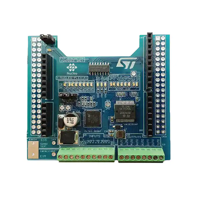
X-NUCLEO-PLC01A1
Industrial input/output expansion board based on VNI8200XP
and CLT01-38SQ7 for STM32 Nucleo
Description
Features
Enables a PLC (Programmable Logic
Controller) function subset on STM32
Nucleo
8x input with CLT01-38SQ7 high-speed
protected digital termination array
8x output with VNI8200XP high-side solid
state relay
Status LEDs: Fault, Thermal, Power
IO (input/output) activity LEDs 24 V power
supply
Free comprehensive development firmware
library and example compatible with
STM32Cube firmware
Compatible with STM32 Nucleo boards
Compatible with Arduino UNO R3 connector
RoHS compliant
July 2015
The X-NUCLEO-PLC01A1 is an industrial
input/output evaluation board which expands the
STM32 Nucleo board functionality with a PLC
(programmable logic controller) function subset. It
is compatible with the Arduino UNO R3
connector layout and is designed around
VNI8200XP (solid state relay) and CLT01-38SQ7
(octal digital termination array). The X-NUCLEOPLC01A1 interfaces with the STM32 MCU via the
SPI peripheral. Moreover, it is equipped with a
set of diagnostic and activity LEDs to facilitate
application debugging. It can accept other
STM32 plug-on expansion boards to further
extend the STM32 Nucleo board functionality.
The X-NUCLEO-PLC01A1 allows the rapid
evaluation of the ICs on board performing a basic
set of PLC operations in conjunction with the XCUBE-PLC1 software package. X-NUCLEOPLC01A1 is not intended to evaluate the single
devices at their full specifications. VNI8200XP
includes advanced protection and fault detection
features. CLT01-38SQ7 provides protection and
isolation in industrial operating conditions as well
as an 'energy-less' status indication for each of
the eight input channels, featuring minimal power
consumption; it is designed for situations that are
required to pass the IEC61000-4-2 8 kV and
15 kV test standards. Both the CLT01-38SQ7
and the VNI8200XP are designed to meet the
most common industrial requirements (i.e.
IEC61000-4-2, IEC61000-4-4, IEC61000-4-5 or
IEC61131-2); to eveluate them further, refer to
the single-product evaluation boards, available at
www.st.com.
DocID028022 Rev 1
1/7
www.st.com
�Schematic diagrams
1
X-NUCLEO-PLC01A1
Schematic diagrams
Figure 1: X-NUCLEO-PLC01A1 schematic, part 1
Morpho Connectors
CN7
1
3
5
7
9
11
13
15
17
19
21
23
25
27
29
31
33
35
37
CN10
2
4
6
8
10
12
14
16
18
20
22
24
26
28
30
32
34
36
38
C1
+3V3
NRST
+3V3
5V
C2
1
3
D15
5
D14
AVDD 7
9
D13 11
D12 13
D11 15
D10 17
19
D9
21
D8
23
D7
25
D6
27
D5
29
D4
31
D3
33
D2
35
D1
37
D0
100nF
100nF
VIN
A0
A1
A2
A3
A4
A5
Morpho_Connector
2
4
6
8
10
12
14
16
18
20
22
24
26
28
30
32
34
36
38
Morpho Connector
CN5
Nucleo Connectors
D15
D14
AVDD
CN6
1
2
3
4
5
6
7
8
D13
D12
J5
R1
0E
NRST
+3V3
5V
1
2
VCC_uc
R2
0E
D11
D10
D9
R3
0E
SPI_SCK
R5
0E
SPI_MISO
SPI_MOSI
SPI_CS2
VIN
D8
R4
0E
10
9
8
7
6
5
4
3
2
1
HEADER 10
SPI_CS1
HEADER 8
CN8
CN9
1
2
3
4
5
6
A0
A1
A2
A3
A4
A5
R6
0E
D7
D6
R13
0E
D5
D4
D3
DNM
HEADER 6
SPI_SCK
HEADER 8
Note :-- Al l Resisto rs in this section should be SMD080 5
SPI activity LEDs
SPI Activity LED
R15
330R
SPI_SCK
D2
DNM
DNM
2/7
DocID028022 Rev 1
D2
D1
D0
OUT_EN
8
7
6
5
4
3
2
1
�X-NUCLEO-PLC01A1
Schematic diagrams
Figure 2: X-NUCLEO-PLC01A1 schematic, part 2
47K
15k
R25
R26
CLT01-38SQ7
R27
0E
CLT_CS1
CLT_SCK
R28
CLT_MISO
VDD_CLT
LED1
D13
LED3
D15
LED5
D17
LED7
220R
CLT_CS1
LED2
D12
LED4
D14
C3
LED6
D16
33pF
LED8
D18
CS1
3
J11
CLT01-38SQ7
LED6
LED7
LED8
NC
NC
COMp
NC
NC
NC
NC
NC
NC
36
35
34
33
32
31
30
29
28
27
26
25
R39
220R
CLT_SCK
SCK
C13
33pF
CLT_IN5
CLT_IN6
CLT_IN7
CLT_IN8
R41
220R
CLT_MISO
MISO
Vc
C14
33pF
Vcs
Input
J8
1
2
3
4
5
6
7
8
9
10
Vinput 24V
R29 2K2
R30
2K2
R33
2K2
R35
2K2
R37
CLT_IN1 C4
CLT_IN2
CLT_IN3 C6
CLT_IN4
CLT_IN5 C8
CLT_IN6
CLT_IN7 C11
CLT_IN8
2K2
R32
R34
R36
2K2
2K2
2K2
22nF
C5
22nF
C7
22nF
C10
22nF
C12
22nF
22nF
22nF
22nF
Input_Connector
PGND
2K2
Vinput
TP3
1
TP2
+24V
1
1
U1
CLT_IN1
CLT_IN2
CLT_IN3
CLT_IN4
10K
VDD
DVR
NC
SPM
NC
NC
NC
COMp
NC
NC
NC
NC
Vc
Vcs
COMp
IN1
IN2
IN3
IN4
COMp
IN5
IN6
IN7
IN8
R40
1
2
3
4
5
6
7
8
9
10
11
12
13
14
15
16
17
18
19
20
21
22
23
24
VDD_CLT
0E
2
R38
SUB
CS
SCK
MOSI
NC
MISO or /MISO
COMs
REF
LED1
LED2
LED3
LED4
LED5
49
48
47
46
45
44
43
42
41
40
39
38
37
C9
100nF/10V
D11
R42
Vc
1M5 R43
Vcs
C15
4n7/3kV-N.M.
D19
SM15T33CA
C19
4n7/3kV-N.M.
C16
1uF/50V
+
C17
100uF/50V
C18
33nF/50V
R44
120K
PGND
PGND
PGND
D20
STPS1H100A
PGND
DocID028022 Rev 1
3/7
�DocID028022 Rev 1
C45
33p F /10V
M ISO
CS 2
SC K
M OSI
CS 1
R57
R56
R52
R50
220 R
220 R
220 R
220 R
VNI_W D
VNI_M IS O
33p F/10V
C44
V NI_ C S 2
33p F/10V
C40
VNI_S CK
33p F/10V
C25
VNI_M OS I
33p F/ 10V
C20
VNI_OU T _E N
220 R
33p F/10V
100p F
R 51
C47
10K
+5V 0
10nF/10V
10nF/10V
+5V0
C39
100p F
C48
C38
100 nF / 10V
C27
47K
R49
10K
R48
R47
10K
C 26
+5V 0
R 46
+5V0
ROW 3
ROW 2
ROW 1
ROW 0
CO L 1
COL0
VNI_M IS O
VNI_CS2
VNI_S CK
VNI_M OS I
V N I _W D
100p F
C 46
1
2
3
4
5
6
7
8
9
10
11
12
13
14
15
16
17
18
TP4
+24V
C21
NC
NC
O UT 1
O UT 2
O UT 3
O UT 4
O UT 5
O UT 6
O UT 7
O UT 8
NC
BOO T
PHAS E
GND
FB
T W ARN
FAULT
PG
VNI8200XP
SE L2
SE L1 /IN1
W D_EN/IN2
O UT _EN/IN3
W D/IN4
SDI/IN5
CLK/IN6
SS /IN7
SDO /IN8
VREG
CO L0
CO L1
DC VDD
VREF
RO W 0
RO W 1
RO W 2
RO W 3
U2
1
220 R
37
4/7
TAB /V CC
R45
PG
/FA ULT
/T W ARN
FB
10k
LE D
LE D
D24
680 R
D23
R60
FB
680 R
LE D
1
R 55
10nF/10V
R 59
+5V 0
T P5
C33
680 R
+5V 0
BA T 48
D21
R 54
100 uH
L1
22nF/50V
R 58
C 28
D 22
+5V 0
PG
/FA ULT
/T W ARN
100p F/50V
C43
36
35
34
33
32
31
30
29
28
27
26
25
24
23
22
21
20
19
1uF/50V
C41
470 nF/10V
3K3
2K
R53
C29
C30
C 34
C 31
C35
C32
C 36
J10
Output_Connector
C37
P GND
22nF/50V
22nF/50V
22nF/50V
22nF/50V
22nF/ 50V
22nF/50V
22nF/50V
22nF/50V
4.7uF/10V
C42
+5V0
1
2
3
4
5
6
7
8
Schematic diagrams
Figure 3: X-NUCLEO-PLC01A1 schematic, part 3
X-NUCLEO-PLC01A1
VNI8200XP
�X-NUCLEO-PLC01A1
Schematic diagrams
Figure 4: X-NUCLEO-PLC01A1 schematic, part 4
OUTPUT LEDs
R61
COL0
COL1
680R
R62
680R
R63
680R
R64
680R
R65
ROW0
D25
LED1
D26
LED2
D27
LED3
D28
LED4
D29
LED5
D30
LED6
D31
LED7
D32
LED8
ROW1
680R
R66
680R
R67
680R
R68
ROW2
ROW3
680R
Digital isolator
VCC_uc
+5V0
C22
C24
C23
10uF/6.3V
100nF/10V
100nF/10V
VCC_uc
+5V0
U3
SPI_MOSI
SPI_SCK
SPI_CS1
SPI_CS2
OUT_EN
SPI_MISO
1
2
3
4
5
6
7
8
VDD1
A1
A2
A3
A4
A5
A6
GND1
VDD2
B1
B2
B3
B4
B5
B6
GND2
16
15
14
13
12
11
10
9
MOSI
SCK
CS1
CS2
VNI_OUT_EN
MISO
Si8661
DocID028022 Rev 1
5/7
�Revision history
2
X-NUCLEO-PLC01A1
Revision history
Table 1: Document revision history
6/7
Date
Version
17-Jul-2015
1
DocID028022 Rev 1
Changes
Initial release.
�X-NUCLEO-PLC01A1
IMPORTANT NOTICE – PLEASE READ CAREFULLY
STMicroelectronics NV and its subsidiaries (“ST”) reserve the right to make changes, corrections, enhancements, modifications, and
improvements to ST products and/or to this document at any time without notice. Purchasers should obtain the latest relevant information on ST
products before placing orders. ST products are sold pursuant to ST’s terms and conditions of sale in place at the time of order
acknowledgement.
Purchasers are solely responsible for the choice, selection, and use of ST products and ST assumes no liability for application assistance or the
design of Purchasers’ products.
No license, express or implied, to any intellectual property right is granted by ST herein.
Resale of ST products with provisions different from the information set forth herein shall void any warranty granted by ST for such product.
ST and the ST logo are trademarks of ST. All other product or service names are the property of their respective owners.
Information in this document supersedes and replaces information previously supplied in any prior versions of this document.
© 2015 STMicroelectronics – All rights reserved
DocID028022 Rev 1
7/7
�