Part Number: XRNI30W-1
Phototransistor
Features
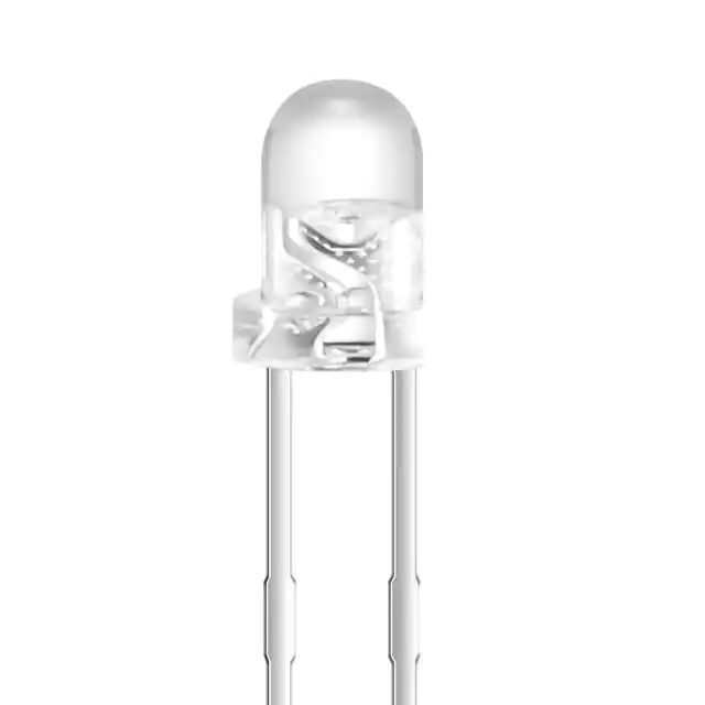
Package Schematics
● Radial / Through hole package
● Reliable & robust
● Low power consumption
● RoHS Compliant
Notes:
1. All dimensions are in millimeters (inches).
2. Tolerance is ±0.25(0.01") unless otherwise noted.
3. Specifications are subject to change without notice.
Electrical / Optical Characteristics at TA=25°C
Symbol
Parameter
Min.
Typ.
Max.
Unit
Test Condiction
VBR CEO
Collector-to-Emitter Breakdown Voltage
30
-
-
V
IC = 100µA
Ee = 0mW/cm2
VBR ECO
Emitter-to-Collector Breakdown Voltage
5
-
-
V
IE = 100µA
Ee = 0mW/cm2
VCE(SAT)
Collector-to-Emitter Saturation Voltage
-
-
0.8
V
IC = 2mA
Ee = 20mW/cm2
ICEO
Collector Dark Current
-
-
100
nA
VCE = 10V
Ee = 0mW/cm2
TR
Rise Time (10% to 90%)
-
15
-
µs
TF
Fall Time (90% to 10%)
-
15
-
µs
0.3
0.8
-
mA
VCE = 5V
Ee = 1mW/cm2
λ= 940nm
420
-
1120
nm
-
-
940
-
nm
-
-
50
-
deg
-
I(ON)
On State Collector Current
λ0.1
Range of spectral bandwidth
λp
Wavelength of peak sensitivity
2θ1/2
Angle of half sensitivity
VCE = 5V
IC = 1mA
RL = 1KΩ
Absolute Maximum Ratings at TA=25°C
Parameter
Maximum Ratings
Collector-to-Emitter Voltage
30V
Emitter-to-Collector Voltage
5V
Power Dissipation at (or below) 25°C Free Air Temperature
Operating / Storage Temperature Range
Lead Solder Temperature (>5mm for 5sec)
100mW
-40 ~ +85°C
260°C
A Relative Humidity between 40% and 60% is recommended in
ESD-protected work areas to reduce static build up during assembly process (Reference JEDEC/JESD625-A and JEDEC/J-STD-033)
Dec 18,2020
XDSA3288
V7
Layout: Maggie L.
P. 1/3
�Part Number: XRNI30W-1
100%
Ta = 25 °C
15°
Ta = 25 °C
80%
0°
1.0
30°
60%
45°
40%
60°
0.5
20%
75°
0%
350
450
550
650
750
850
Wavelength (nm)
950
1050
1150
90°
0°
Relative Intensity Vs. CIE Wavelength
1
Collector current (mA)
VCE = 5V
Ta = 25 °C
1
0.1
Collector dark current (nA)
0.8
2
Ee = 1mW/cm
0.6
0.4
2
Ee = 0.5mW/cm
0.2
Ee = 0.25mW/cm2
0
0.1
1
10
Irradiance Ee (mW/cm2)
Collector Current vs.
Irradiance
1000
VCE = 20V
Ee = 0
100
10
1
0.1
0
25
50
75
100
Ambient temperature (°C)
Collector Dark Current vs.
Ambient Temperature
Dec 18,2020
Ta = 25 °C
30°
160
45°
60°
75°
0.0
90°
125
100
75
50
25
0
VCE=5V
140
Ee=1mW/cm2
120
100
80
60
40
20
0
0
1
2
3
4
5
Collector-emitter voltage VCE (V)
Collector Current vs.
Collector-Emitter Voltage
0
Collector dark current (nA)
0.01
0.01
Collector power dissipation Pd (mW)
Collector current Ic (mA)
10
15°
Spatial Distribution
Relative collector current (%)
Relative spectral sensitivity (a. u.)
Phototransistor
20
40
60
80 100
Ambient temperature (°C)
Relative Collector Current vs.
Ambient Temperature
10
Ta = 25 °C
1
0.1
0.01
0
20
40
60
80 100
Ambient temperature (°C)
Collector Power Dissipation vs.
Ambient Temperature
0
5
10 15 20 25 30
Collector-emitter voltage VCE (V)
Collector Dark Current vs.
Collector-Emitter Voltage
XDSA3288
V7
Layout: Maggie L.
P. 2/3
�Part Number: XRNI30W-1
Phototransistor
PACKING & LABEL SPECIFICATIONS
TERMS OF USE
1. Data presented in this document reflect statistical figures and should be treated as technical reference only.
2. Contents within this document are subject to improvement and enhancement changes without notice.
3. The product(s) in this document are designed to be operated within the electrical and environmental specifications indicated on the datasheet.
User accepts full risk and responsibility when operating the product(s) beyond their intended specifications.
4. The product(s) described in this document are intended for electronic applications in which a person’s life is not reliant upon the LED. Please
consult with a SunLED representative for special applications where the LED may have a direct impact on a person’s life.
5. The contents within this document may not be altered without prior consent by SunLED.
6. Additional technical notes are available at https://www.SunLEDusa.com/TechnicalNotes.asp
Dec 18,2020
XDSA3288
V7
Layout: Maggie L.
P. 3/3
�
很抱歉,暂时无法提供与“XRNI30W-1”相匹配的价格&库存,您可以联系我们找货
免费人工找货- 国内价格 香港价格
- 1+3.535461+0.45797
- 10+2.4203510+0.31352
- 100+1.71881100+0.22265
- 500+1.40141500+0.18154
- 1000+1.296831000+0.16799
- 2000+1.207802000+0.15646
- 5000+1.110265000+0.14382
- 10000+1.0493410000+0.13593
- 25000+0.9828125000+0.12731