IRF830
POWER MOSFET
GENERAL DESCRIPTION
This Power MOSFET is designed for low voltage, high speed power switching applications such as switching regulators, conveters, solenoid and relay drivers.
FEATURES
Higher Current Rating Lower rDS(ON), Lower Capacitances Lower Total Gate Charge Tighter VSD Specifications Avalanche Energy Specified
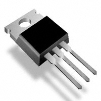
PIN CONFIGURATION
TO-220/TO-220FP
SYMBOL
D
Top View
G ATE
SO URCE
DRAIN
G
S
1 2 3
N-Channel MOSFET
ORDERING INFORMATION
Part Number .................IRF830FP Package TO-220FP .................IRF830....................................................TO-220
ABSOLUTE MAXIMUM RATINGS
Rating Drain to Current Continuous Pulsed (Note 1) Gate-to-Source Voltage Total Power Dissipation Derate above 25 Single Pulse Avalanche Energy (Note 2) Operating and Storage Temperature Range Thermal Resistance Junction to Case Junction to Ambient Maximum Lead Temperature for Soldering Purposes, 1/8” from case for 10 seconds EAS TJ, TSTG
JC JA
Symbol ID IDM VGS PD
Value 5.0 18 ±20 96 0.77 125 -55 to 150 1.70 62 300
Unit A V W W/ mJ /W
Continue
TL
Page 1
�IRF830
POWER MOSFET
ELECTRICAL CHARACTERISTICS
Unless otherwise specified, TJ = 25 .
CIRF830 Characteristic Drain-Source Breakdown Voltage (VGS = 0 V, ID = 250 A) Drain-Source Leakage Current (VDS = 500V, VGS = 0 V) Gate-Source Leakage Current-Forward (Vgsf = 20 V, VDS = 0 V) Gate-Source Leakage Current-Reverse (Vgsr = -20 V, VDS = 0 V) Gate Threshold Voltage (VDS = VGS, ID = 250 A) Static Drain-Source On-Resistance (VGS = 10 V, ID = 2.7A) (Note 3) Forward Transconductance (VDS = 15V, ID = 2.5 A) (Note 3) Input Capacitance Output Capacitance Reverse Transfer Capacitance Turn-On Delay Time Rise Time Turn-Off Delay Time Fall Time Total Gate Charge Gate-Source Charge Gate-Drain Charge (VDS = 400V, ID = 5A VGS = 10 V) (Note 3) (VDD = 250 V, ID = 5 A, RG = 9.1 , VGS = 10 V) (Note 3) (VDS = 25 V, VGS = 0 V, f = 1.0 MHz) Symbol V(BR)DSS IDSS 25 IGSSF IGSSR VGS(th) RDS(on) gFS Ciss Coss Crss td(on) tr td(off) tf Qg Qgs Qgd LD LS 2.8 520 170 11 7.0 9.0 20 10 10 2 3 4.5 7.5 730 240 20 10 20 40 20 2.0 100 -100 4.0 1.5 mhos pF pF pF ns ns ns ns nC nC nC nH nH nA nA V Min 500 Typ Max Units V A
Internal Drain Inductance (Measured from the drain lead 0.25” from package to center of die) Internal Drain Inductance (Measured from the source lead 0.25” from package to source bond pad) SOURCE-DRAIN DIODE CHARACTERISTICS Reverse Recovery Charge Forward Turn-On Time Reverse Recovery Time Diode Forward Voltage IS = 5A, VGS = 0 V IF = 5A, di/dt = 100A/µs , TJ = 25
Qrr ton trr VSD
1.8 ** 415 1.5
µC ns V
Note (1) Repetitive rating; pulse width limited by max. junction temperature (2) VDD = 100V, VGS = 10V, L=10mH, IAS = 5A, RG = 25 (3) Pulse.Test:.Duty Cycle 2% , Pulse.Width 300µs ** Negligible, Dominated by circuit inductance
P
Page 2
�IRF830
POWER MOSFET
TYPICAL ELECTRICAL CHARACTERISTICS
Page 3
�IRF830
POWER MOSFET
PACKAGE DIMENSION
TO-220
D A
φ
F E
c1
PIN 1: GATE PIN 2: DRAIN PIN 3: SOURCE
E1
A A1 b b1 c c1 D E E1 e e1 F L L1
L1
L
e b1 e1 Front View b
A1 c Side View
φ
TO-220FP
C
J
D
Q
H
R1 .5 0
R1 .5 0
B
.1 ²0 .18 R3
0
I
A B
A
C D E
E
P
K O
G H I J K M N O P Q
0 .6 R1
G
b
R b b1 b2 e
b1 e Front View
b2 R
N M
Side View
Back View
Page 4
�
很抱歉,暂时无法提供与“IRF830”相匹配的价格&库存,您可以联系我们找货
免费人工找货