09-Aug.-2016 Ver.1.3
EYSGJNZXX, EYSGJNZWY
TAIYO YUDEN
Bluetooth ® low energy Module
Bluetooth® 4.2 low energy
EYSGJNZXX (16kB RAM)
EYSGJNZWY (32kB RAM)
Data Report
The Bluetooth® word mark and logos are owned by the Bluetooth SIG, Inc. and any use of
such marks by TAIYO YUDEN CO., LTD. is under license.
TAIYO YUDEN
1/31
�09-Aug.-2016 Ver.1.3
EYSGJNZXX, EYSGJNZWY
TAIYO YUDEN
Document constituent list
Control name
Control No.
General Items
Absolute maximum ratings
Electrical characteristics
Circuit schematic
Outline / Appearance
Pin Layout
Handling Precaution
Packaging Specification
Antenna application note
Design guide
Notes
HD-AG-A150049
HD-AM-A150049
HD-AE-A150049
HD-MC-A150049
HD-AD-A150049
HD-BA-A150049
HQ-BA-537
HD-BB-A150049
Document Page
1/5 - 5/5
1/1
1/7 - 7/7
1/3 - 3/3
1/1
1/2 - 2/2
1/2 - 2/2
1/3 - 3/3
1/3 - 3/3
1/1
1/1
Revision History
14-Sep.-2015 > Ver.1.00 Release
21-Dec.-2015 > Ver.1.01 Update
18-Mar.-2016 > Ver.1.1 Update
12-Jul.-2016 > Ver.1.2 Update
09-Aug.-2016 > Ver.1.3 Update
TAIYO YUDEN
2/31
�09-Aug.-2016 Ver.1.3
EYSGJNZXX, EYSGJNZWY
Control No.
HD-AG-A150049
(1/5)
TAIYO YUDEN
Control name
General Items
Scope
This specification (“Specification”) applies to the hybrid IC “EYSGJNZXX” and “EYSGJNZWY”, a
Bluetooth® 4.2 low energy module (“Product”) manufactured by TAIYO YUDEN Co., Ltd. (“TAIYO
YUDEN”)
1. Type: EYSGJN
User Code: EYSGJNZXX (16kB RAM), EYSGJNZWY (32kB RAM)
*User Code may be changed for mass production or other cases.
2. Function:
Radio frequency module.
Bluetooth® standard Ver 4.2 low energy conformity
3. Application: Health & Fitness Equipment, Sensor, Toys
4. Structure:
Hybrid IC loaded with silicon monolithic semiconductor
Compatible with industrial standard reflow profile for Pb-free solders
+6
Can meet with RoHS compliance (Pb, Cd, Hg, Cr , PBB, PBDE)
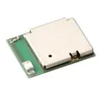
5. Outline: 11.3 x 5.1 x 1.3 mm
28-pin Land Grid Array
6. Marking: Part number, Lot number
7. Features:
- Small outline by PCB substrate
- Low power consumption
- Integrated antenna
- Integrated system clock
- Bluetooth® 4.2 low energy conformity
- Slave or Master Role
8. Packaging:
Packaging method: Tape & reel + aluminum moisture barrier bag
Packaging unit: 2000
*It might be provided as tray at sample stage.
TAIYO YUDEN
3/31
�09-Aug.-2016 Ver.1.3
EYSGJNZXX, EYSGJNZWY
Control No.
HD-AG-A150049
(2/5)
TAIYO YUDEN
Control name
General Items
9. Note:
a. Any question arising from this Specification shall be solved through mutual discussion by the
parties hereof.
b. This Product is not designed to be radiation durable and should not be used under the
circumstance of radiation.
c. The operating conditions of this Product are as shown in this Specification. Please note that
TAIYO YUDEN shall not be liable for a failure and/or abnormality which is caused by use under
the conditions other than the operating conditions hereof.
d. The Product mentioned in this Specification is manufactured for use in Health & Fitness
Equipment, Sensor and Toys. Before using this Product in any special equipment (such as
medical equipment, space equipment, air craft, disaster prevention equipment), where higher
safety and reliability are duly required, the applicability and suitability of this Product must be
fully evaluated by the customer at its sole risk to ensure correct and safe operation of these
special equipments. Also, evaluation of the safety function of this Product even for use in
general electronics equipment shall be thoroughly made and when necessary, a protective
circuit shall be added during the design stage, all at the customer’s sole risk.
e. a) You are requested to fully check and confirm by the start of mass production of this Product
that (1) no bug, defect or other failure is included in firmware incorporated in this Product
(“Incorporated Software”), (2) no bug defect or other failure arising from installation of this
Product in which is contained Incorporated Software into your products is included in
Incorporated Software, and that Incorporated Software fully meets your intended use, although
TAIYO YUDEN sufficiently inspects or verifies quality of Incorporated Software.
b) Please note that TAIYO YUDEN is not responsible for any failure arising out of bugs or
defects in Incorporated Software.
f. TAIYO YUDEN warrants only that this Product is in conformity with this Specification for one
year after purchase and shall in no event give any other warranty.
g. Communication between this Product and others might not be established nor maintained
depending on radio environment or operating conditions of this Product and other Bluetooth®
products.
h. In order to test for Radio Law certification with a device incorporating this module, the Host
Software must be able to put the module into test mode. Please contact TAIYO YUDEN for
further details.
i. This Product operates in the unlicensed ISM band at 2.4GHz. In case this Product is used
around the other wireless devices which operate in same frequency band of this Product, there
is a possibility that interference may occur between this Product and such other devices. If
such interference occurs, please stop the operation of other devices or relocate this Product
before using this Product or do not use this Product around the other wireless devices.
j. Please thoroughly evaluate our module with your products before going mass production.
k. User Code Modification Notice.
User Code for sample modules or part numbers in this Specification are TAIYO YUDEN
standard part numbers. When any modification is made to a module to meet requested
specifications, the part number will be changed. Please contact TAIYO YUDEN to confirm
whether your part number needs to be modified.
Please see the following examples for cases when part numbers are modified:
- for specific firmware version (our standard item firmware will be upgraded occasionally)
- for other relevant cases (specific or different setting, form, sizes, or display etc..)
TAIYO YUDEN
4/31
�09-Aug.-2016 Ver.1.3
EYSGJNZXX, EYSGJNZWY
Control No.
HD-AG-A150049
(3/5)
TAIYO YUDEN
Control name
General Items
l. Alternative components may used to this module. The intended components is used within the
warranty written in this document (characteristics, size, operating condition, reliability, public
regulation such as radio type approval) and Taiyo Yuden confirmed there are not any
problems with the replacement. The traceability of the components is secured each production
lot.
m. Caution for Export Control
This Product may be subject to governmental approvals, consents, licenses, authorizations,
declarations, filings, and registrations for export or re-export of the Product, required by
Japanese Foreign Exchange and Foreign Trade Law (including related laws and regulations)
and/or any other country’s applicable laws or regulations related to export control.
If you plan to export or re-export this Product, it is strongly recommended that you check and
confirm, the necessary procedures to export or re-export of this Product as required by
applicable laws and regulations, and if necessary, you have to obtain necessary and
appropriate approvals or licenses from governmental authority at your own risk and expense.
n. Japan Regulatory Information
This module is approved with the specific antenna on this module.
a) Please ensure that your product can bear a label with the following information. If the
product is so small that it is not practicable to place the label, please place it in the
instruction manual and package. The mark diameter shall be equal or grater than 3mm.
This product installs a radio system which has been approved as a radio station in a
low power data communication system based on the Radio Law.
EYSGJN : 001-A05676
o. Canada Regulatory Information
a) This device complies with Industry Canada license-exempt RSS standards. Operation
is subject to the following two conditions: (1) this device may not cause interference,
and (2) this device must accept any interference, including interference that may cause
undesired operation of the device.
L'utilisation de ce dispositif est autorisée seulement aux conditions suivantes: (1) il ne
doit pas produire de brouillage et (2) l'utilisateur du dispositif doit être prêt à accepter
tout brouillage radioélectrique reçu, même si ce brouillage est susceptible de
compromettre le fonctionnement du dispositif.
b) This product is certified as type of the portable device with Industry Canada Rules. To
maintain compliance with RF Exposure requirement,please use within specification of
this product.
Ce produit est certifié comme type de l'appareil portable avec Industrie Règles de
Canada. Pour maintenir l'acquiescement avec exigence Exposition de RF, veuillez
utiliser dans spécification de ce produit.
- IC: 4389B-EYSGJN
-FVIN : F1
c) Please notify certified ID by either one of the following method on your product.
Specifiez ID certifiée dans votre produit par une de méthode suivante.
-Contains Transmitter module IC : 4389B-EYSGJN
-Contains IC : 4389B-EYSGJN
TAIYO YUDEN
5/31
�09-Aug.-2016 Ver.1.3
EYSGJNZXX, EYSGJNZWY
Control No.
HD-AG-A150049
(4/5)
TAIYO YUDEN
Control name
General Items
p. FCC Regulatory Information
a) This device complies with part 15 of the FCC Rules. Operation is subject to the
following two conditions: (1) This device may not cause harmful interference, and (2)
this device must accept any interference received, including interference that may
cause undesired operation.
b) Please notify certified ID by either one of the following method on your product.
-Contains Transmitter Module FCC ID: RYYEYSGJN
-Contains FCC ID: RYYEYSGJN
c) CAUTION: changes or modifications not expressly approved by the party responsible
for compliance could void the use’s authority to operate the equipment.
d) This product is certified as type of the portable device with FCC Rules. To maintain
compliance with RF Exposure requirement, please use within specification of this
product.
e) The antenna used for this transmitter must not be co-located or operating in
conjunction with any other antenna or transmitter.
q. CE Regulatory Information
a) When your end product installs this module, it is required to proceed additional
certification processes before placing on the market in EU member states to make your
products fully comply with relative EU standards.
b) TAIYO YUDEN can provide you the test reports of conducted measurement portion for
the radio module. You can utilize the test reports for the certification processes of your
end product as it requires radio testing.
r. This Product is designed for use in products which comply with Bluetooth® Specifications (Ver
4.2 LE) (“Bluetooth Specifications”). TAIYO YUDEN disclaims and is not responsible for
any liability concerning infringement by this Product under any intellectual property right
owned by third party in case the customer uses this Product in any product which does not
comply with Bluetooth Specifications (the “non-complying products”). Furthermore, TAIYO
YUDEN warrants only that this Product complies with this Specification and does not grant
any other warranty including warranty for application of the non-complying products.
s. Taiyo Yuden writes firmware for fixed SoftDevice (EYSGJNZXX : S110 V8.0.0,
EYSGJNZWY : S120 V2.1.0) to this product. Customer writes firmware that is match the
customer applications including SoftDevice at the customer's own responsibility.
t. The Electrical Characteristics defined in this Specification are of the module with above
SoftDevice. If other firmware is installed, the characteristics may differ from the defined
value in the Electrical Characteristics. Bluetooth qualification and radio type approval may
become invalid.
u. EYSGJN series module is qualified as PHY only with Component category by Bluetooth SIG.
The QDID of this module is 69825.The final product needs to get qualification as End
product combining with PHY (module), SoftDevice and Profile before selling the product.
The combination of Link and Host layer is differ with SoftDevice. Please refer to following
combination and consult with your qualification body and BQE.
TAIYO YUDEN
6/31
�09-Aug.-2016 Ver.1.3
EYSGJNZXX, EYSGJNZWY
Control No.
HD-AG-A150049
(5/5)
TAIYO YUDEN
Control name
General Items
TAIYO YUDEN
7/31
�09-Aug.-2016 Ver.1.3
EYSGJNZXX, EYSGJNZWY
Control No.
HD-AM-A150049
(1/1)
TAIYO YUDEN
Control name
Absolute maximum ratings
Absolute maximum ratings
Symbol
Parameter
VCC_NRF
Min.
Max.
Units
-0.3
+3.6
V
0
V
GND
VIO
-0.3
VCC_NRF+ 0.3
V
Storage temperature
-40
+85
Deg-C
1
kV
100
V
MSL
Moisture Sensitivity Level
3
ESD HBM
Human Body Model
ESD MM
Machine Model
Endurance
Flash Memory Endurance
20000
Retention
Flash Memory Retention
10 years
write/erase
cycles
At 40 deg-C
Number of times an
address can be written
2
times
between erase cycles
TAIYO YUDEN
8/31
�09-Aug.-2016 Ver.1.3
EYSGJNZXX, EYSGJNZWY
Control No.
HD-AE-A150049
(1/7)
TAIYO YUDEN
Control name
Electrical characteristics
Electrical characteristics
Recommendation operating range
Symbol
Parameter
VCC_NRF
Min.
Typ.
Max.
Units
1.8
3.0
3.6
V
2.1
3.0
3.6
V
100
ms
75
Deg-C
Supply voltage, normal mode
Supply voltage, normal mode,
VCC_NRF
DC/DC converter output voltage 1.9 V
tR_VCC_NRF
Supply rise time (0V to 1.8V)*1
TA
Operation temperature
-25
25
*1 The on-chip power-on reset circuitry may not function properly for rise times outside the specified
interval. Also after power off, it must start up from below 0.3V. The on-chip power-on
reset circuitry may not function properly.
DC Specifications
The Specification applies for Topr.= 25 degrees C, VCC_NRF = 3.0V
Max.
Units
VIH
Symbol
Input high voltage
0.7 VCC_NRF
VCC_NRF
V
VIL
Input low voltage
GND
0.3 VCC_NRF
V
VOH
Output high voltage (std. drive, 0.5 mA)
VCC_NRF-0.3
VCC_NRF
V
VOH
Output high voltage (high-drive, 5 mA)
VCC_NRF-0.3
VCC_NRF
V
VOL
Output low voltage (std. drive, 0.5 mA)
GND
0.3
V
VOL
Output low voltage (high-drive, 5 mA)
GND
0.3
V
RPU
Pull-up resistance
11
13
16
kohm
RPD
Pull-down resistance
11
13
16
kohm
ITX,+4dBm
TX only run current @ POUT =+4 dBm
16
mA
ITX,0dBm
TX only run current @ POUT = 0 dBm
10.5
mA
IRX
RX only run current
13
mA
0.6
uA
0.6
uA
2.6
uA
IOFF
IOFF,8k
ION
Parameter (condition)
Min.
Current in SYSTEM-OFF, no RAM
retention
Current in SYSTEM-OFF
mode 8 kB SRAM retention
SYSTEM-ON base current
Typ.
Note that when you use the RC oscillator, it will increase around 10uA of average power
consumption compared to a 32.768kHz crystal.
TAIYO YUDEN
9/31
�09-Aug.-2016 Ver.1.3
EYSGJNZXX, EYSGJNZWY
Control No.
HD-AE-A150049
(2/7)
TAIYO YUDEN
Control name
Electrical characteristics
UART specifications
TAIYO YUDEN
10/31
�09-Aug.-2016 Ver.1.3
EYSGJNZXX, EYSGJNZWY
Control No.
HD-AE-A150049
SPI Slave specifications
(3/7)
TAIYO YUDEN
Control name
Electrical characteristics
TAIYO YUDEN
11/31
�09-Aug.-2016 Ver.1.3
EYSGJNZXX, EYSGJNZWY
Control No.
HD-AE-A150049
SPI Master specifications
(4/7)
TAIYO YUDEN
Control name
Electrical characteristics
TAIYO YUDEN
12/31
�09-Aug.-2016 Ver.1.3
EYSGJNZXX, EYSGJNZWY
Control No.
HD-AE-A150049
(5/7)
TAIYO YUDEN
Control name
Electrical characteristics
TWI specifications
TAIYO YUDEN
13/31
�09-Aug.-2016 Ver.1.3
EYSGJNZXX, EYSGJNZWY
Control No.
HD-AE-A150049
(6/7)
TAIYO YUDEN
Control name
Electrical characteristics
GPIOTE specifications
RF Specifications
Symbol
Description
Min.
Fop
Operating frequencies
2402
Typ.
PLLres
PLL programming resolution
Df
Frequency deviation
PRF
Maximum output power
PRFC
RF power control range
PRFCR
RF power accuracy
PWHISP
RF power whisper mode
-30
PBW
20 dB bandwidth for modulated carrier
950
PRF1
Max.
Units
2480
MHz
1
+/-225
20
+/-250
MHz
+/-275
kHz
4
dBm
24
dB
+/-4
dB
dBm
1100
kHz
1st Adjacent Channel Transmit Power 1 MHz
-20
dBc
PRF2
2nd Adjacent Channel Transmit Power 2 MHz
-45
dBc
PRXMAX
Maximum received signal strength at < 0.1% PER
0
dBm
PSENS IT
Receiver sensitivity (0.1% BER) Ideal transmitter
-93
dBm
PSENS DT
Receiver sensitivity (0.1% BER) dirty transmitter
-91
dBm
TAIYO YUDEN
14/31
�09-Aug.-2016 Ver.1.3
EYSGJNZXX, EYSGJNZWY
Control No.
HD-AE-A150049
(7/7)
TAIYO YUDEN
Control name
Electrical characteristics
DFU Specifications
TAIYO YUDEN
15/31
�09-Aug.-2016 Ver.1.3
EYSGJNZXX, EYSGJNZWY
Control No.
HD-MC-A150049
(1/3)
TAIYO YUDEN
Control name
Circuit Schematic
Block Diagram
VCC_NRF
AVDD
DCC
DEC2
nRF51822
WLCSP
OUT_ANT
OUT_MOD
SWDCLK
SWDIO/RESET
Filter
X'tal 32MHz
P0.00 to P0.06
P0.17, P0.19,
P0.21, P0.23,
P0.25
P0.26_XL2
P0.27_XL1
TAIYO YUDEN
16/31
�09-Aug.-2016 Ver.1.3
EYSGJNZXX, EYSGJNZWY
Control No.
HD-MC-A150049
(2/3)
TAIYO YUDEN
Control name
Circuit Schematic
Sample circuits
TAIYO YUDEN
17/31
�09-Aug.-2016 Ver.1.3
EYSGJNZXX, EYSGJNZWY
Control No.
HD-MC-A150049
(3/3)
TAIYO YUDEN
Control name
Circuit Schematic
Reference Circuits
SWDIO is also system reset
(active low).
FC-12M (EPSON)
NX2012SA (NDK)
CL=12.5pF
P0.00-P0.27 are GPIOs. By
setting in the application
software, it is assigned to pin
any such as UART, etc. Please
make Open Status about
unused pins.
VIO is connected to VCC in a
module. Please use IO
voltage under the following
conditions.
Input high (V): 0.7VCC to VCC
Input low (V): GND to 0.3VCC
SWD (Serial Wire Debug) is a
high-performance 2-pin debug
port low-pin-count alternative to
JTAG. It can write the application
software and firmware by those
pins through the J-Link Lite.
Example and Applications written
for Keil uVision IDE.
When the customers use the
cable in Nordic DK to use J-LINK
Lite, it will need to implement the
socket on the customers main
board side. The socket will be
"10-pin connector two rows of
1.27mm pitch (Ex:
PSS-720153-05, Hirosugi
instrument). The cable in Nordic
DK has a protection to avoid
reverse connection. In order to
use this cable, please remove the
pin 7 of the socket on main
board.
J-Link Lite is working with 3.3V. It
does not work with 1.8V.
In order to use the built-in
antenna on the module,
please connect PAD13
and PAD14 as short as
possible.
In case of the operation with the
battery, we recommend that you
add a capacitor of about 100uF in
view of the voltage drop during
TX/RX
In case of the power supply
voltage fluctuation by the load
change is large, the module may
not function properly.
If an external regulator is used,
the load change characteristic
should be good in order to keep
stable voltage as possible when
the current is change.
TAIYO YUDEN
18/31
�09-Aug.-2016 Ver.1.3
EYSGJNZXX, EYSGJNZWY
Control No.
HD-AD-A150049
(1/1)
TAIYO YUDEN
Control name
Outline/Appearance
Tolerance: +/- 0.2mm
Unit : (mm)
The dimension of the land pattern is the same as a foot pattern.
Recommended metal mask for solder printing
Pad size
Metal mask opening
Signal pad 23 – 0.4 x 0.8 mm
0.35 x 0.7 mm
Corner pad 4 – 0.55 x 0.8 mm
0.45 x 0.75 mm
Center pad 1 – 2.8 x 1.5 mm
1.1 x 1.2 mm x 2
0.4
The metal mask thickness: t=0.1mm
1.1
Center pad
1.2
TAIYO YUDEN
19/31
�09-Aug.-2016 Ver.1.3
EYSGJNZXX, EYSGJNZWY
Control No.
HD-BA-A150049
(1/2)
TAIYO YUDEN
Control name
Pin Layout
Pin Descriptions
Pin
Pin name
Pin
function
Ground
Description
1
GND
2
P0.27
AIN1
XL1
General purpose I/O pin
Digital I/O
ADC input 1
Analog input
Crystal connection for 32.768kHz crystal oscillator or
Analog input
external 32.768kHz crystal reference
3
P0.26
AIN0
XL2
Digital I/O
General purpose I/O pin
Analog input
ADC input 0
Analog
Crystal connection for 32.768kHz crystal oscillator
output
4
P0.21
Digital I/O
General purpose I/O pin
5
VCC_NRF
Power
Power supply
6
AVDD
Power
Analog Power supply
7
P0.23
Digital I/O
General purpose I/O pin
8
P0.17
Digital I/O
General purpose I/O pin
9
GND
Ground
Ground (0 V)
10
DEC2
Power
Power supply for low voltage mode
11
P0.19
Digital I/O
General purpose I/O pin
12
GND
Ground
Ground (0 V)
13
OUT_ANT
Antenna
In/Out
Internal antenna. It should be connected to Pin 14 OUT_MOD for
normal operation.
14
OUT_MOD RF In/Out
RF I/O pin. It should be connected to Pin 13 OUT_ANT for normal
operation.
15
GND
Ground
Ground (0 V)
16
SWDIO
Digital I/O
System reset (active low). Also HW debug and flash programming
I/O
17
SWDCLK
Digital input
HW debug and flash programming I/O
18
P0.25
Digital I/O
General purpose I/O pin
19
P0.03
AIN4
Digital I/O
General purpose I/O pin
Analog input ADC input 4
20
GND
Ground
21
P0.01
AIN2
Digital I/O
General purpose I/O pin
Analog input ADC input 2
22
P0.02
AIN3
Digital I/O
General purpose I/O pin
Analog input ADC input 3
Ground (0 V)
Ground (0 V)
TAIYO YUDEN
20/31
�09-Aug.-2016 Ver.1.3
EYSGJNZXX, EYSGJNZWY
Control No.
HD-BA-A150049
(2/2)
TAIYO YUDEN
Control name
Pin Layout
Pin
Pin name
23
P0.00
AREF0
Pin
Description
function
Digital I/O
General purpose I/O pin
Analog input ADC Reference voltage
24
DCC
Power
25
P0.05
AIN6
Digital I/O
General purpose I/O pin
Analog input ADC input 6
26
P0.06
AIN7
AREF1
Digital I/O
General purpose I/O pin
Analog input ADC input 7
Analog input ADC Reference voltage
27
P0.04
AIN5
Digital I/O
General purpose I/O pin
Analog input ADC input 5
28
GND
Ground
DC/DC output
Ground (0 V)
TAIYO YUDEN
21/31
�09-Aug.-2016 Ver.1.3
EYSGJNZXX, EYSGJNZWY
TAIYO YUDEN
Control No.
Control name
HQ-BA-537
(1/2)
Handling Precaution
This specification describes desire and conditions especially for mounting.
Desire/Conditions
(1)
Environment conditions for use and storage
1. Store the components in an environment of < 40deg-C/90%RH if they are in a moisture
barrier bag packed by TAIYO YUDEN.
2. Keep the factory ambient conditions at < 30deg-C/60%RH .
3. Store the components in an environment of < 25±5deg-C/10%RH after the bag is opened.
(The condition is also applied to a stay in the manufacture process).
(2)
Conditions for handling of products
Make sure all of the moisture barrier bags have no holes, cracks or damages at receiving. If
an abnormality is found on the bag, its moisture level must be checked in accordance with 2
in (2).
Refer to the label on the bag.
1. All of the surface mounting process (reflow process) must be completed in 12 months
from the bag sea date.
2. Make sure humidity in the bag is less than 10%RH immediately after open, using a
humidity indicator card sealed with the components.
3. All of the surface mounting process (reflow process including rework process) must be
completed in 168 hours after the bag is opened (inclusive of any other processes).
4. If any conditions in (1) or condition 2 and 3 in (2) are not met, bake the components in
accordance with the conditions at 125deg-C 24hours
5. As a rule, baking the components in accordance with conditions 4 in (2) shall be once.
6. Since semi-conductors are inside of the components, they must be free from static
electricity while handled.(