®
SEMICONDUCTOR
200mW SOD-323 SURFACE MOUNT
Small Outline Flat Lead Plastic Package
Zener Voltage Regulators
Absolute Maximum Ratings
Symbol
PD
Green Product
TA = 25°C unless otherwise noted
Parameter
Value
Units
200
mW
Power Dissipation
TSTG
Storage Temperature Range
-65 to +150
°C
TOPR
Operating Temperature Range
-65 to +150
°C
These ratings are limiting values above which the serviceability of the diode may be impaired.
SOD-323 Flat Lead
Specification Features:
Wide Zener Voltage Range Selection, 2.0V to 75V
VZ Tolerance Selection of ±5% (C Series)
Cathode
RoHS Compliant
Anode
Green EMC
ELECTRICAL SYMBOL
Matte Tin(Sn) Lead Finish
Band Indicates Cathode
Weight: approx. 0.004g
AEC-Q101 Qualified
Electrical Characteristics
TA = 25°C unless otherwise noted
VZ @ IZT
(Volts)
IZT
(mA)
ZZT @ IZT
()
Max
IZK
(mA)
ZZK @ IZK
()
Max
IR @ VR
(A)
Max
VR
(Volts)
2.10
5
100
1
564
120
0.5
2.2
2.31
5
100
1
564
120
0.7
2.4
2.52
5
100
1
564
45
1
2.57
2.7
2.84
5
100
1
564
18
1
Z2
2.85
3.0
3.15
5
100
1
564
9
1
MM3Z3V3CW
Z3
3.14
3.3
3.47
5
95
1
564
4.5
1
MM3Z3V6CW
Z4
3.42
3.6
3.78
5
90
1
564
4.5
1
MM3Z3V9CW
Z5
3.71
3.9
4.10
5
90
1
564
2.7
1
MM3Z4V3CW
Z6
4.09
4.3
4.52
5
90
1
564
2.7
1
MM3Z4V7CW
Z7
4.47
4.7
4.94
5
80
1
470
2.7
2
MM3Z5V1CW
Z8
4.85
5.1
5.36
5
60
1
451
1.8
2
MM3Z5V6CW
Z9
5.32
5.6
5.88
5
40
1
376
0.9
2
MM3Z6V2CW
ZA
5.89
6.2
6.51
5
10
1
141
2.7
4
MM3Z6V8CW
ZB
6.46
6.8
7.14
5
15
1
75
1.8
4
MM3Z7V5CW
ZC
7.11
7.5
7.86
5
15
1
75
0.9
5
MM3Z8V2CW
ZD
7.79
8.2
8.61
5
15
1
75
0.63
5
MM3Z9V1CW
ZE
8.65
9.1
9.56
5
15
1
94
0.45
6
MM3Z10VCW
ZF
9.50
10
10.50
5
20
1
141
0.18
7
MM3Z11VCW
ZG
10.45
11
11.55
5
20
1
141
0.09
8
MM3Z12VCW
ZH
11.40
12
12.60
5
25
1
141
0.09
8
Device
Type
Device
Marking
Min
Nom
Max
MM3Z2V0CW
Z+
1.90
2.0
MM3Z2V2CW
Z⊥
2.09
MM3Z2V4CW
Z0
2.28
MM3Z2V7CW
Z1
MM3Z3V0CW
Number: DB-087
April 2019, Revision F
Page 1
MM3Z2V0CW through MM3Z75VCW
TAK CHEONG
�TAK CHEONG
®
SEMICONDUCTOR
Electrical Characteristics
TA = 25°C unless otherwise noted
VZ @ IZT
(Volts)
IZT
(mA)
ZZT @ IZT
()
Max
IZK
(mA)
ZZK @ IZK
()
Max
13.65
5
30
1
160
0.09
8
15
15.75
5
30
1
188
0.045
10.5
15.20
16
16.80
5
40
1
188
0.045
11.2
ZM
17.10
18
18.90
5
45
1
212
0.045
12.6
ZN
19.00
20
21.00
5
55
1
212
0.045
14.0
MM3Z22VCW
ZP
20.90
22
23.10
5
55
1
235
0.045
15.4
MM3Z24VCW
ZR
22.80
24
25.20
5
70
1
235
0.045
16.8
MM3Z27VCW
ZS
25.65
27
28.35
2
80
0.5
282
0.045
18.9
MM3Z30VCW
ZT
28.50
30
31.50
2
80
0.5
282
0.045
21.0
MM3Z33VCW
ZU
31.35
33
34.65
2
80
0.5
306
0.045
23.0
MM3Z36VCW
ZV
34.20
36
37.80
2
90
0.5
329
0.045
25.2
MM3Z39VCW
ZW
37.05
39
40.95
2
130
0.5
329
0.045
27.3
MM3Z43VCW
ZX
40.85
43
45.15
2
150
0.5
353
0.045
30.1
MM3Z47VCW
ZY
44.65
47
49.35
2
170
0.5
353
0.045
33.0
MM3Z51VCW
Z−
48.45
51
53.55
2
180
0.5
376
0.045
35.7
MM3Z56VCW
Z=
53.20
56
58.80
2
200
0.5
400
0.045
39.2
MM3Z62VCW
Z≡
58.90
62
65.10
2
215
0.5
423
0.045
43.4
MM3Z68VCW
Z>
64.60
68
71.40
2
240
0.5
447
0.045
47.6
MM3Z75VCW
Z<
71.25
75
78.75
2
255
0.5
470
0.045
52.5
Device
Type
Device
Marking
Min
Nom
Max
MM3Z13VCW
ZJ
12.35
13
MM3Z15VCW
ZK
14.25
MM3Z16VCW
ZL
MM3Z18VCW
MM3Z20VCW
IR @ VR
(A)
Max
VR
(Volts)
VF Forward Voltage = 1 V Maximum @ IF = 10 mA for all types
Notes:
1.
2.
3.
4.
The Zener Voltage (VZ) is tested under pulse condition of 10mS.
The device numbers listed have a standard tolerance on the nominal zener voltage of ±5%.
For detailed information on price, availability and delivery of nominal zener voltages between the voltages shown and tighter
voltage tolerances, contact your nearest Tak Cheong Electronics representative.
The zener impedance is derived from the 60-cycle ac voltage, which results when an ac current having an rms value equal to
10% of the dc zener current (IZT or IZK) is superimposed to IZT or IZK.
Number: DB-087
April 2019, Revision F
Page 2
�TAK CHEONG
®
SEMICONDUCTOR
RATING AND CHARACTERISTIC CURVES
Fig.2 EFFECT OF ZENER VOLTAGE ON ZENER IMPEDANCE
Fig.1 TYPICAL FORWARD VOLTAGE
POWER PASSIPATION,mW
250
200
150
100
50
0
0
25
50
75
100
125
150
175
200
TEMPERATURE [℃]
Fig.3 POWER DISSIPATION VS. AMBIENT TEMP.
Fig.5 ZENER BREAKDOWN CHARACTERISTICS
Fig.4 TYPICAL CAPACITANCE
Fig.6 ZENER BREAKDOWN CHARACTERISTICS
Number: DB-087
April 2019, Revision F
Page 3
�TAK CHEONG
®
SEMICONDUCTOR
Fig.7 TYPICAL LEAKGE CURRENT
SOD-323 Package Outline
NOTES:
1. The above package outline is similar to JEITA SC-90.
2. Dimensions are exclusive of Burrs, Mold Flash & Tie Bar extrusions.
Number: DB-087
April 2019, Revision F
Page 4
�TAK CHEONG
®
DISC LA IMER NOTIC E
NOTICE
The information presented in this document is for reference only. Tak Cheong reserves the right to make
changes without notice for the specification of the products displayed herein.
The product listed herein is designed to be used with ordinary electronic equipment or devices, and not
designed to be used with equipment or devices which require high level of reliability and the malfunction of
with would directly endanger human life (such as medical instruments, transportation equipment, aerospace
machinery, nuclear-reactor controllers, fuel controllers and other safety devices), Tak Cheong
Semiconductor Co., Ltd., or anyone on its behalf, assumes no responsibility or liability for any damagers
resulting from such improper use of sale.
This publication supersedes & replaces all information previously supplied. For additional information, please
visit our website http://www.takcheong.com, or consult your nearest Tak Cheong’s sales office for further
assistance.
“AEC-Q101 QUALIFIED” Statement:
Tak Cheong has the capabilities to conduct tests for product packages by grouping in selective bases. Tak
Cheong reserves the rights for making necessary arrangement for the subject test due to the amount of time
and resources involved.
Number: DB-317
April 01, 2019 / A
�
很抱歉,暂时无法提供与“MM3Z2V2CW”相匹配的价格&库存,您可以联系我们找货
免费人工找货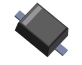


 工商网监
湘ICP备2023018690号
工商网监
湘ICP备2023018690号
