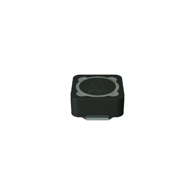
SMT power inductors
Size 12.5 x 12.5 x 6 (mm)
Series/Type:
B82477P2
Date:
August 2023
TDK Electronics AG 2023. Reproduction, publication and dissemination of this publication, enclosures hereto
and the information contained therein without TDK Electronics’ prior express consent is prohibited.
�SMT power inductors
Size 12.5 x 12.5 x 6 (mm)
B82477P2
Rated inductance 1 ... 1000 µH
Rated current 0.53 ... 9.25 A
Construction
Ferrite core
Magnetically shielded
Winding: enamel copper wire
Winding soldered to terminals
Injection molded base
Features
High mechanical stability
Temperature range up to +150 °C
High rated current
Low DC resistance
Suitable for lead-free reflow soldering as referenced in JEDEC J-STD 020
Qualification to AEC-Q200
RoHS-compatible
Applications
Filtering of supply voltages
Coupling, decoupling
DC/DC converters
Automotive electronics
Terminals
Base material Cu
Layer composition Ni, Sn (lead-free)
Electro-plated
Marking
Marking on component:
Manufacturer, L value (μH, coded), manufacturing date (YWWD)
Minimum data on reel:
Manufacturer, ordering code, L value, quantity, date of packing
Delivery mode and packing units
24-mm blister tape, wound on 330-mm reel
Packing unit: 600 pcs./reel
Please read Cautions and warnings and
Important notes at the end of this document.
2
8/23
�SMT power inductors
Size 12.5 x 12.5 x 6 (mm)
B82477P2
Dimensional drawing and layout recommendation
Dimensions in mm
Taping and packing
Blister tape
Reel
Dimensions in mm
Please read Cautions and warnings and
Important notes at the end of this document.
3
8/23
�SMT power inductors
Size 12.5 x 12.5 x 6 (mm)
B82477P2
Technical data and measuring conditions
Rated inductance LR
Operating temperature range
Thermal rated current Ith
Saturation current ISat
DC resistance Rtyp
Solderability (lead-free)
Resistance to soldering heat
Climatic category
Storage conditions
Weight
Measured with LCR meter Keysight E4980 or equivalent at
frequency fL, 0.1 V, room temperature
−55 °C … +150 °C
Max. permissible DC with temperature increase of ≤ 40 K
at rated temperature
Max. permissible DC with inductance decrease L/L0 of
approx. 10%
Measured at room temperature
Dip and look method Sn95.5Ag3.8Cu0.7:
+(245 ±5) °C, (3 ±0.3) s
Wetting of soldering area ≥ 90%
(based on IEC 60068-2-58)
As referenced in JEDEC J-STD 020
55/150/56 (to IEC 60068-1)
Mounted: –55 °C … +150 °C
Packaged: –25 °C … +40 °C, ≤ 75% RH
Approx. 3.3 g
Please read Cautions and warnings and
Important notes at the end of this document.
4
8/23
�SMT power inductors
Size 12.5 x 12.5 x 6 (mm)
B82477P2
Characteristics and ordering codes
LR
Tolerance
fL
Ith
Isat
Rmax
MHz
A
A
0.1
9.25
10.0
0.008
B82477P2102M000
1.5
0.1
8.70
8.70
0.010
B82477P2152M000
2.2
0.1
7.20
8.00
0.012
B82477P2222M000
3.3
0.1
6.70
7.20
0.014
B82477P2332M000
4.7
0.1
5.40
5.70
0.016
B82477P2472M000
6.8
0.1
4.80
4.80
0.020
B82477P2682M000
10
0.1
4.30
4.00
0.025
B82477P2103M000
15
0.1
3.70
3.30
0.030
B82477P2153M000
22
0.1
3.40
2.80
0.036
B82477P2223M000
33
0.1
2.70
2.20
0.055
B82477P2333M000
47
0.1
2.40
1.90
0.070
B82477P2473M000
68
0.1
1.85
1.50
0.110
B82477P2683M000
100
0.1
1.65
1.30
0.140
B82477P2104M000
150
0.1
1.35
1.00
0.210
B82477P2154M000
220
0.1
1.15
0.80
0.300
B82477P2224M000
330
0.1
0.95
0.68
0.460
B82477P2334M000
470
0.1
0.80
0.58
0.550
B82477P2474M000
680
0.1
0.62
0.48
1.050
B82477P2684M000
1000
0.1
0.53
0.40
1.300
B82477P2105M000
H
1.0
20% ≙ M
Please read Cautions and warnings and
Important notes at the end of this document.
5
8/23
Ordering code
�SMT power inductors
Size 12.5 x 12.5 x 6 (mm)
B82477P2
Inductance L versus DC load current IDC
measured with LCR meter Keysight E4980 or
equivalent, typical values at room temperature
Please read Cautions and warnings and
Important notes at the end of this document.
Current derating Iop/IR
versus ambient temperature TA
6
8/23
�SMT power inductors
Size 12.5 x 12.5 x 6 (mm)
B82477P2
Cautions and warnings
Please note the recommendations in our Inductors data book (latest edition), online catalogs and
in the data sheets.
– Particular attention should be paid to the derating curves, if given. Derating applies in the case
the ambient temperature in application exceeds the rated temperature of the component.
– Ensure the operation temperature of the component in application not to exceed the maximum
specified value or the upper climatic category temperature.
– The soldering conditions should also be observed. Temperatures quoted in relation to wave
soldering refer to the pin, not the housing.
If the components are to be washed varnished it is necessary to check whether the washing varnish agent that is used has a negative effect on the wire insulation, any plastics that are used, or
on glued joints. It is possible for washing varnish agent residues to have a negative effect in the
long−term on wire insulation.
Washing processes may damage the product due to the possible static or cyclic mechanical
loads (e.g., ultrasonic cleaning). They may cause cracks to develop on the product and its parts,
which might lead to reduced reliability or lifetime.
The following points must be observed if the components are potted, sealed, or varnished in customer applications:
– Many potting, sealing, or varnishing materials shrink as they harden. They therefore exert a
pressure on the plastic housing or core. This pressure can have a deleterious effect on electrical properties, and in extreme cases can damage the core or plastic housing mechanically.
– It is necessary to check whether the potting, sealing or varnishing materials used attack or destroy the wire insulation, plastics, or glue.
– The effect of the potting, sealing, or varnishing materials may change the high−frequency behavior of the components.
Magnetic core materials such as ferrites are sensitive to direct impact. This can cause the core
material to flake or lead to breakage of the magnetic core material.
Any type of tension or pressure on the product may result in damage and affect its functionality
and reliability.
– The products are only to be attached to fixings or mounting holes provided for this purpose in
accordance with the data sheet.
– If additional mechanical forces are applied to the component, e.g., application of gap pads, it
is necessary to check whether they attack or destroy any part of the component.
– It is not permitted for the product specified in the data sheet to assume a mechanical function
in the final application.
Inductance value can drop if external metallic or magnetic parts will be put close to the coil or into
the air gap of the coil or core or magnetic material.
Even for customer-specific products, conclusive validation of the component in the circuit can
only be carried out by the customer.
Display of ordering codes for TDK Electronics products
The ordering code for one and the same product can be represented differently in data sheets, data
books, other publications, on the company website, or in order-related documents such as shipping
notes, order confirmations and product labels. The varying representations of the ordering
codes are due to different processes employed and do not affect the specifications of the
respective products. Detailed information can be found on the Internet under
www.tdk-electronics.tdk.com/orderingcodes.
Please read Cautions and warnings and
Important notes at the end of this document.
7
8/23
�Important notes
The following applies to all products named in this publication:
1. Some parts of this publication contain statements about the suitability of our products for
certain areas of application. These statements are based on our knowledge of typical requirements that are often placed on our products in the areas of application concerned. We nevertheless expressly point out that such statements cannot be regarded as binding statements
about the suitability of our products for a particular customer application. As a rule, we
are either unfamiliar with individual customer applications or less familiar with them than the customers themselves. For these reasons, it is always ultimately incumbent on the customer to
check and decide whether a product with the properties described in the product specification is
suitable for use in a particular customer application.
2. We also point out that in individual cases, a malfunction of electronic components or failure before the end of their usual service life cannot be completely ruled out in the current
state of the art, even if they are operated as specified. In customer applications requiring a
very high level of operational safety and especially in customer applications in which the malfunction or failure of an electronic component could endanger human life or health (e.g. in accident prevention or life-saving systems), it must therefore be ensured by means of suitable design of the customer application or other action taken by the customer (e.g. installation of protective circuitry or redundancy) that no injury or damage is sustained by third parties in the event
of malfunction or failure of an electronic component.
3. The warnings, cautions and product-specific notes must be observed.
4. In order to satisfy certain technical requirements, some of the products described in this publication may contain substances subject to restrictions in certain jurisdictions (e.g. because they are classed as hazardous). Useful information on this will be found in our Material
Data Sheets on the Internet (www.tdk-electronics.tdk.com/material). Should you have any more
detailed questions, please contact our sales offices.
5. We constantly strive to improve our products. Consequently, the products described in this
publication may change from time to time. The same is true of the corresponding product
specifications. Please check therefore to what extent product descriptions and specifications
contained in this publication are still applicable before or when you place an order.
We also reserve the right to discontinue production and delivery of products. Consequently, we cannot guarantee that all products named in this publication will always be available. The
aforementioned does not apply in the case of individual agreements deviating from the foregoing
for customer-specific products.
6. Unless otherwise agreed in individual contracts, all orders are subject to our General Terms
and Conditions of Supply.
8
8/23
�Important notes
7. Our manufacturing sites serving the automotive business apply the IATF 16949 standard.
The IATF certifications confirm our compliance with requirements regarding the quality management system in the automotive industry. Referring to customer requirements and customer specific requirements (“CSR”) TDK always has and will continue to have the policy of respecting individual agreements. Even if IATF 16949 may appear to support the acceptance of unilateral requirements, we hereby like to emphasize that only requirements mutually agreed upon can
and will be implemented in our Quality Management System. For clarification purposes we
like to point out that obligations from IATF 16949 shall only become legally binding if individually
agreed upon.
8. The trade names EPCOS, CarXield, CeraCharge, CeraDiode, CeraLink, CeraPad, CeraPlas,
CSMP,
CTVS, DeltaCap, DigiSiMic, FilterCap, FormFit, InsuGate, LeaXield, MediPlas,
MiniBlue, MiniCell, MKD, MKK, ModCap, MotorCap, PCC, PhaseCap, PhaseCube, PhaseMod,
PhiCap, PiezoBrush, PlasmaBrush, PowerHap, PQSine, PQvar, SIFERRIT, SIFI, SIKOREL,
SilverCap, SIMDAD, SiMic, SIMID, SineFormer, SIOV, ThermoFuse, WindCap, XieldCap are
trademarks registered or pending in Europe and in other countries. Further information will be
found on the Internet at www.tdk-electronics.tdk.com/trademarks.
Release 2023-08
9
8/23
�