Hardware
Documentation
D at a S h e e t
®
HAL 1002
Highly Precise Programmable
Hall-Effect Switch
Edition Sept. 3, 2019
DSH000163_003EN
�HAL 1002
DATA SHEET
Copyright, Warranty, and Limitation of Liability
The information and data contained in this document are believed to be accurate and
reliable. The software and proprietary information contained therein may be protected
by copyright, patent, trademark and/or other intellectual property rights of
TDK-Micronas. All rights not expressly granted remain reserved by TDK-Micronas.
TDK-Micronas assumes no liability for errors and gives no warranty representation or
guarantee regarding the suitability of its products for any particular purpose due to
these specifications.
By this publication, TDK-Micronas does not assume responsibility for patent infringements or other rights of third parties which may result from its use. Commercial conditions, product availability and delivery are exclusively subject to the respective order
confirmation.
Any information and data which may be provided in the document can and do vary in
different applications, and actual performance may vary over time.
All operating parameters must be validated for each customer application by customers’
technical experts. Any mention of target applications for our products is made without a
claim for fit for purpose as this has to be checked at system level.
Any new issue of this document invalidates previous issues. TDK-Micronas reserves
the right to review this document and to make changes to the document’s content at any
time without obligation to notify any person or entity of such revision or changes. For
further advice please contact us directly.
Do not use our products in life-supporting systems, military, aviation, or aerospace
applications! Unless explicitly agreed to otherwise in writing between the parties,
TDK-Micronas’ products are not designed, intended or authorized for use as components in systems intended for surgical implants into the body, or other applications
intended to support or sustain life, or for any other application in which the failure of the
product could create a situation where personal injury or death could occur.
No part of this publication may be reproduced, photocopied, stored on a retrieval system or transmitted without the express written consent of TDK-Micronas.
TDK-Micronas Trademarks
– HAL
TDK-Micronas Patents
US 6 968 484, EP 1 039 357, EP 1 575 013, EP 1 949 034
Third-Party Trademarks
All other brand and product names or company names may be trademarks of their
respective companies.
TDK-Micronas GmbH
Sept. 3, 2019; DSH000163_003EN
2
�HAL 1002
DATA SHEET
Contents
Page
Section
Title
4
5
5
1.
1.1.
1.2.
Introduction
Major Applications
Features
6
6
2.
2.1.
Ordering Information
Device-Specific Ordering Codes
7
7
9
15
17
3.
3.1.
3.2.
3.3.
3.4.
Functional Description
General Function
Digital Signal Processing and EEPROM
General Calibration Procedure
Example: Calibration of a Position Switch
19
19
23
23
23
24
24
25
26
27
4.
4.1.
4.2.
4.3.
4.4.
4.5.
4.6.
4.7.
4.8.
4.9.
Specifications
Outline Dimensions
Soldering, Welding and Assembly
Pin Connections and Short Descriptions
Dimension of Sensitive Area
Absolute Maximum Ratings
Storage and Shelf Life
Recommended Operating Conditions
Characteristics
Magnetic Characteristics
28
28
29
31
31
5.
5.1.
5.2.
5.3.
5.4.
Application Notes
Application Circuit
Temperature Compensation
Ambient Temperature
EMC and ESD
32
32
32
35
36
37
40
6.
6.1.
6.2.
6.3.
6.4.
6.5.
6.6.
Programming
Definition of Programming Pulses
Definition of the Telegram
Telegram Codes
Number Formats
Register Information
Programming Information
41
7.
Document History
TDK-Micronas GmbH
Sept. 3, 2019; DSH000163_003EN
3
�HAL 1002
DATA SHEET
Highly Precise Programmable Hall-Effect Switch
Release Note: Revision bars indicate significant changes to previous version
1. Introduction
The HAL1002 is the improved successor of the HAL 1000 Hall-effect switch. The major
sensor characteristics, the two switching points BON and BOFF , are programmable for
the application. The sensor can be programmed to be unipolar or latching, sensitive to
the magnetic north pole or sensitive to the south pole, with normal or with an electrically
inverted output signal. Several examples are shown in Fig. 3–4 through Fig. 3–7.
The HAL1002 is based on the HAL83x family and features a temperature-compensated
Hall plate with chopper offset compensation, an A/D converter, digital signal processing, a
push-pull output stage, an EEPROM memory with redundancy and Lock function for the
calibration data, a serial interface for programming the EEPROM, and protection devices
at all pins. Internal digital signal processing is of great benefit because analog offsets, temperature shifts, and mechanical stress effects do not degrade the sensor accuracy.
The HAL1002 is programmable by modulating the supply voltage. No additional programming pin is needed. Programming is simplified through the use of a two-point calibration. Calibration is accomplished by adjusting the sensor output directly to the input
signal. Individual adjustment of each sensor during the customer’s manufacturing process is possible. With this calibration procedure, the tolerances of the sensor, the magnet, and the mechanical positioning can be compensated for the final assembly. This
offers a low-cost alternative for all applications that presently require mechanical adjustment or other system calibration.
In addition, the temperature compensation of the Hall-effect Integrated Circuit (IC) can
be tailored to all common magnetic materials by programming first and second order
temperature coefficients of the Hall-effect sensor’s sensitivity. This enables operation
over the full temperature range with constant switching points.
The calculation of the individual sensor characteristics and the programming of the
EEPROM memory can easily be done with a PC and the application kit from
TDK-Micronas.
The sensor is designed and produced in sub-micron CMOS technology for the use in
hostile industrial and automotive applications with nominal supply voltage of 5 V in the
ambient temperature range from 40 °C up to 150 °C.
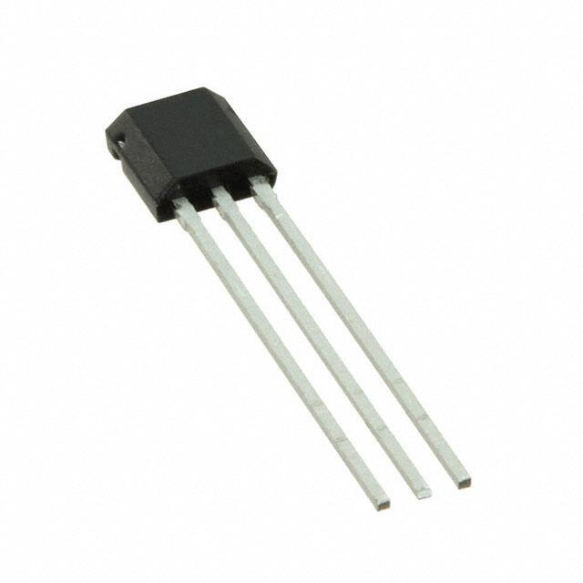
The HAL1002 is available in the leaded package TO92UT.
TDK-Micronas GmbH
Sept. 3, 2019; DSH000163_003EN
4
�HAL 1002
DATA SHEET
1.1. Major Applications
Due to the sensor’s versatile programming characteristics, the HAL1002 is a potential
solution for applications which require very precise contactless switching:
– Endpoint detection
– Level switch (e.g. liquid level)
– Electronic fuse (current measurement)
1.2. Features
– High-precision Hall-effect switch with programmable switching points and switching
behavior
– AEC-Q100 qualified
– EMC and ESD optimized design
ESD HBM performance >7 kV
– Switching points programmable from 150 mT up to 150 mT in steps of 0.5% of the
magnetic-field range
– Multiple programmable magnetic characteristics in a non-volatile memory (EEPROM)
with redundancy and Lock function
– Temperature characteristics are programmable for matching all common magnetic
materials
– Programming through modulation of the supply voltage
– Operates from 40 °C up to 150 °C ambient temperature
– Operates from 4.5 V up to 8.5 V supply voltage in specification and functions up to 11 V
– Operates with static magnetic fields and dynamic magnetic fields up to 2 kHz
– Extremely robust magnetic characteristics against mechanical stress
– Overvoltage and reverse-voltage protection at all pins
– Short-circuit protected push-pull output
TDK-Micronas GmbH
Sept. 3, 2019; DSH000163_003EN
5
�HAL 1002
DATA SHEET
2. Ordering Information
A Micronas device is available in a variety of delivery forms. They are distinguished by a
specific ordering code:
XXX NNNN PA-T-C-P-Q-SP
Further Code Elements
Temperature Range
Package
Product Type
Product Group
Fig. 2–1: Ordering code principle
For a detailed information, please refer to the brochure:
“Sensors and Controllers: Ordering Codes, Packaging, Handling”.
2.1. Device-Specific Ordering Codes
HAL 1002 is available in the following package and temperature variants.
Table 2–1: Available packages
Package Code (PA)
Package Type
UT
TO92UT-1 (spread)
UT
TO92UT-2 (in-line)
Table 2–2: Available temperature ranges
Temperature Code (T)
Temperature Range
A
TJ = 40 °C to 170 °C
The relationship between ambient temperature (TA) and junction temperature (TJ) is
explained in Section 5.3. on page 31.
For available variants for Configuration (C), Packaging (P), Quantity (Q), and Special
Procedure (SP) please contact TDK-Micronas.
Table 2–3: Available ordering codes and corresponding package marking
Available Ordering Code
Package Marking
HAL 1002UT-A-[C-P-Q-SP]
1002A
TDK-Micronas GmbH
Sept. 3, 2019; DSH000163_003EN
6
�HAL 1002
DATA SHEET
3. Functional Description
3.1. General Function
The HAL1002 is a monolithic Integrated Circuit (IC) which provides a digital output signal in response to an magnetic input signal. The sensor is based on the HAL83x
design.
The Hall plate is sensitive to magnetic north and south polarity. The external magneticfield component perpendicular to the branded side of the package generates a Hall voltage. This voltage is converted to a digital value and processed in the Digital Signal Processing unit (DSP) according to the settings of the EEPROM registers. The function and
the parameters for the DSP are explained in Section 3.2. on page 9.
The setting of the LOCK register disables the programming of the EEPROM memory for
all time. This register cannot be reset.
As long as the LOCK register is not set, the output characteristic can be adjusted by
programming the EEPROM registers. The IC is addressed by modulating the supply
voltage (see Fig. 3–1). After detecting a command, the sensor reads or writes the memory and answers with a digital signal on the output pin. The output of the sensor does
react to a magnetic field during the communication.
Internal temperature compensation circuitry and the spinning current offset compensation
enable the operation over the full temperature range with minimal changes of the switching
points. The circuitry also rejects offset shifts due to mechanical stress from the package.
The non-volatile memory consists of redundant EEPROM cells. In addition, the HAL1002
is equipped with devices for overvoltage and reverse-voltage protection at all pins.
HAL
1002
VSUP
VOUT (V)
VSUP (V)
8
7
6
5
VSUP
OUT
GND
Fig. 3–1: Programming with VSUP modulation
TDK-Micronas GmbH
Sept. 3, 2019; DSH000163_003EN
7
�HAL 1002
DATA SHEET
VSUP
Internally
stabilized
Supply and
Protection
Devices
Switched
Hall Plate
Temperature
Dependent
Bias
A/D
Converter
Protection
Devices
Oscillator
Digital
Signal
Processing
Digital
Output
100
OUT
EEPROM Memory
Supply
Level
Detection
Lock Control
GND
Fig. 3–2: HAL1002 block diagram
ADC-Readout Register
14 bits
Digital Signal Processing
Digital Output
14 bits
Limiter
A/D
Converter
TC
TCSQ
5 bits
3 bits
Digital
Filter
Mode Register
Range
Filter
3 bits
2 bits
Multiplier
Adder
Comparator
Sensitivity
14 bits
VOQ
11 bits
Low
Level
8 bits
High
Level
9 bits
Lock
Micronas
1 bit
Register
Other: 5 bit
TC Range Select 2 bits
EEPROM Memory
Lock
Control
Fig. 3–3: Details of EEPROM registers and digital signal processing
TDK-Micronas GmbH
Sept. 3, 2019; DSH000163_003EN
8
�HAL 1002
DATA SHEET
3.2. Digital Signal Processing and EEPROM
Note
In this section the digital signal processing is described for a linear sensor
on which the HAL1002 is based.
The DSP is the main part of the sensor and performs the signal processing. The parameters for the DSP are stored in the EEPROM registers. The details are shown in Fig. 3–3.
Terminology:
SENSITIVITY: name of the register or register value
Sensitivity: name of the parameter
EEPROM Registers:
The EEPROM registers include three groups:
Group 1 contains the registers for the adaptation of the sensor to the magnetic system:
MODE for selecting the magnetic-field range and filter frequency, TC and TCSQ for the
temperature characteristics of the magnetic sensitivity and thereby for the switching points.
Group 2 contains the registers for defining the switching points: SENSITIVITY, VOQ,
LOW-LEVEL, and HIGH-LEVEL.
The comparator compares the processed signal voltage with the reference values LowLevel and High-Level.
The output switches on (low) if the signal voltage is higher than the High-Level, and
switches off (high) if the signal falls below the Low-Level. Several examples of different
switching characteristics are shown in Fig. 3–4 to Fig. 3–7.
– The parameter VOQ (Output Quiescent Voltage) corresponds to the signal voltage at
B = 0 mT.
– The parameter Sensitivity defines the magnetic sensitivity:
Sensitivity =
VSignal
B
– The signal voltage can be calculated as follows:
VSignal Sensitivity B + VOQ
Therefore, the switching points are programmed by setting the SENSITIVITY, VOQ,
LOW-LEVEL, and HIGH-LEVEL registers. The available TDK-Micronas software calculates the best parameter set respecting the ranges of each register.
Group 3 contains TDK-Micronas registers and LOCK for the locking of all registers. The
TDK-Micronas registers are programmed and locked during production and are readonly for the customer. These registers are used for oscillator frequency trimming, A/D
converter offset compensation, and several other special settings.
TDK-Micronas GmbH
Sept. 3, 2019; DSH000163_003EN
9
�HAL 1002
DATA SHEET
Digital
Output
Digital
Output
High-Level
High-Level
VOQ
Low-Level
Low-Level
VOQ
B
B
VOUT
VOUT
VDD
VDD
B
B
Fig. 3–4: HAL 1002 with unipolar behavior
Fig. 3–5: HAL1002 with latching behavior
Digital
Output
Digital
Output
VOQ
High-Level
High-Level
Low-Level
Low-Level
VOQ
B
B
VOUT
VOUT
VDD
VDD
B
B
Fig. 3–6: HAL 1002 with unipolar inverted
behavior
TDK-Micronas GmbH
Fig. 3–7: HAL 1002 with unipolar
behavior sensitive to the other magnetic
polarity
Sept. 3, 2019; DSH000163_003EN
10
�HAL 1002
DATA SHEET
MODE register
The MODE register contains all bits used to configure the A/D converter and the different output modes.
Table 3–1: MODE register
MODE
Bit Number
9
8
7
6
Parameter
RANGE
Reserved
OUTPUTMODE
5
4
3
FILTER
2
1
RANGE
(together
with bit 9)
0
Reserved
Magnetic Range
The RANGE bits define the magnetic-field range of the A/D converter.
Table 3–2: RANGE bits
Magnetic Range
RANGE
MODE [9]
MODE [2:1]
±15 mT
1
00
±30 mT
0
00
±60 mT
0
01
±80 mT
0
10
±100 mT
0
11
±150 mT
1
11
Filter
The FILTER bits define the 3 dB frequency of the digital low pass filter.
Table 3–3: FILTER bits
3 dB Frequency
MODE [4:3]
80 Hz
00
500 Hz
10
1 kHz
11
2 kHz
01
TDK-Micronas GmbH
Sept. 3, 2019; DSH000163_003EN
11
�HAL 1002
DATA SHEET
Output Format
The OUTPUTMODE bits define the different output modes of HAL 83x.
Table 3–4: Output formats
Output Format
MODE [7:5]
Switch (positive polarity)
100
Switch (negative polarity)
101
TC Register
The temperature dependence of the magnetic sensitivity can be adapted to different
magnetic materials in order to compensate for the change of the magnetic strength with
temperature. The adaptation is done by programming the TC (Temperature Coefficient)
and the TCSQ registers (Quadratic Temperature Coefficient). Thereby, the slope and the
curvature of the temperature dependence of the magnetic sensitivity can be matched to
the magnet and the sensor assembly. As a result, the output voltage characteristic can
be constant over the full temperature range. The sensor can compensate for linear
temperature coefficients ranging from about 3100 ppm/K up to 1000 ppm/K and
quadratic coefficients from about 7 ppm/K² to 2 ppm/K².
The full TC range is separated in the following four groups:
Table 3–5: TC register
TC-Register
Bit Number
9
Parameter
TC-RANGE
8
7
6
5
4
TC
3
2
1
0
TCSQ
Table 3–6: TC ranges
TC Range [ppm/k]
TC-Range Group
3100 to 1800 (not for ±15 mT range)
0
1750 to 550 (not for ±15 mT range)
2
500 to +450 (default value)
1
+450 to +1000
3
TC (5 bits) and TCSQ (3 bits) have to be selected individually within each of the four
ranges. For example 0 ppm/k requires TC-Range = 1, TC = 15 and TCSQ = 1. Please
refer to Section 5.2. on page 29 for more details.
TDK-Micronas GmbH
Sept. 3, 2019; DSH000163_003EN
12
�HAL 1002
DATA SHEET
Sensitivity Register
The SENSITIVITY register contains the parameter for the multiplier in the DSP. Sensitivity
is programmable between 4 and 4 in steps of 0.00049.
VOQ Register
The VOQ register contains the parameter for the adder in the DSP. VOQ is the signal
voltage without external magnetic field (B = 0 mT, respectively ADC-READOUT = 0)
and programmable from VSUP up to VSUP. For VSUP = 5 V, the register can be
changed in steps of 4.9 mV.
Note
If VOQ is programmed to a negative voltage, the maximum signal voltage is
limited to:
VSignal max = VOQ + VSUP
Reference Level Register
The LOW-LEVEL and HIGH-LEVEL registers contain the reference values of the comparator.
The Low-Level is programmable between 0 V and VSUP/2. The register can be changed
in steps of 9.77 mV. The High-Level is programmable between 0 V and VSUP in steps of
9.77 mV.
The four parameters Sensitivity, VOQ, Low-Level, and High-Level define the switching
points BON and BOFF. For calibration in the system environment, a two-point adjustment
procedure is recommended (see Section 3.3.). The suitable parameter set for each
sensor can be calculated individually by this procedure.
GP Register
This register can be used to store information, like production date or customer serial
number. TDK-Micronas will store production lot number, wafer number and x,y coordinates in registers GP1 to GP3. The total register contains four blocks (GP0 to GP3) with
a length of 13 bits each. The customer can read out this information and store it in his
production data base for reference or he can store own production information instead.
Note
This register is not a guarantee for traceability because readout of registers
is not possible after locking the IC.
To read/write this register it is mandatory to read/write all GP register one
after the other starting with GP0. In case of a writing the registers it necessary to first write all registers followed by one store sequence at the end.
Even if only GP0 should be changed all other GP registers must first be
read and the read out data must be written again to these registers.
TDK-Micronas GmbH
Sept. 3, 2019; DSH000163_003EN
13
�HAL 1002
DATA SHEET
LOCK Register
By setting the LSB of this 2-bit register, all registers will be locked, and the sensor will
no longer respond to any supply voltage modulation. This bit is active after the first
power-off and power-on sequence after setting the Lock bit.
Warning
This register cannot be reset!
ADC-READOUT Register
This 14-bit register delivers the actual digital value of the applied magnetic field after filtering but before the signal processing. This register can be read out and is the basis for
the calibration procedure of the sensor in the system environment.
Digital Output
This 14-bit register delivers the actual value of the applied magnetic field after the signal
processing.
This register can be read out and is the basis for the calibration procedure of the sensor
in the system environment.
Note
The MSB and LSB are reversed compared with all the other registers.
Please reverse this register after readout.
Note
During calibration it is mandatory to set the parameter for OUTPUT MODE
to 0. The Digital Output register can be read out only in this configuration.
For other configurations of the OUTPUT MODE the result read back from
the sensor will be 0. After the calibration the output format can than easily
be switched to the wanted output mode.
TDK-Micronas GmbH
Sept. 3, 2019; DSH000163_003EN
14
�HAL 1002
DATA SHEET
3.3. General Calibration Procedure
For calibration in the system environment, the application kit from TDK-Micronas is recommended. It contains the hardware for the generation of the serial telegram for programming and the corresponding software for the input or calculation of the register values.
In this section, the programming of the sensor using this tool is explained. Please refer
to Section 6. on page 32 for information about programming without this tool.
For the individual calibration of each sensor in the customer‘s application, a two-point
adjustment is recommended (see Fig. 3–8 for an example). When using the application
kit, the calibration can be done in three steps:
Step 1: Input of the registers which need not be adjusted individually
The magnetic circuit, the magnetic material with its temperature characteristics, and the
filter frequency, are given for this application.
Therefore, the values of the following registers should be identical for all sensors in the
application.
– FILTER
(according to maximum signal frequency)
The 500 Hz range is recommended for highest accuracy.
– RANGE
(according to the maximum magnetic field at the sensor position)
– TC and TCSQ
(depends on the material of the magnet and the other temperature dependencies of
the application)
Write the appropriate settings into the HAL1002 registers.
TDK-Micronas GmbH
Sept. 3, 2019; DSH000163_003EN
15
�HAL 1002
DATA SHEET
Step 2: Initialize DSP
As the Digital Output register value depends on the setting of SENSITIVITY, VOQ and
HIGH/LOW LEVEL, these registers have to be initialized with defined values first:
– VOQINITIAL = 2048
– SensINITIAL = (see Table 3–7)
– Low Level = 0
– High Level = 511
Table 3–7: Values for SensINITIAL
3 dB filter frequency
Register value for SensINITIAL (decimal)
80 Hz
950
500 Hz
614
1 kHz
657
2 kHz
1313
Note
This step is done by TDK-Micronas’ customer software automatically by
clicking the Write and Store button.
Step 3: Calculation of the Sensor Parameters
Fig. 3–8 shows the typical characteristics for a contactless switch. There is a mechanical range where the sensor must be switched high and where the sensor must be
switched low.
Set the system to the calibration point where the sensor output must be high, and click
the button “Readout BOFF”. The result is the corresponding digital value.
Then, set the system to the calibration point where the sensor output must be low, click
the button “Readout BON” and get the second digital value.
Now, adjust the hysteresis to the desired value. The hysteresis is the difference
between the switching points and suppresses oscillation of the output signal. With
100% hysteresis, the sensor will switch low and high exactly at the calibration points. A
lower value will adjust the switching points closer together. Fig. 3–8 shows an example
with 80% hysteresis.
By clicking the button “calibrate and store”, the software will calculate the corresponding
parameters for Sensitivity, VOQ, Low-Level, High-Level and stores these values in the
EEPROM.
This calibration must be done individually for each sensor.
The sensor is now calibrated for the customer application. However, the programming
can be changed again if necessary.
TDK-Micronas GmbH
Sept. 3, 2019; DSH000163_003EN
16
�HAL 1002
DATA SHEET
VOUT
Sensor
switched off
Hysteresis
Sensor
switched on
(here 80 %)
position
Calibration points
Fig. 3–8: Characteristics of a position switch
Step 4: Locking the Sensor
The last step is activating the Lock function with the “Lock” button. The sensor is now
locked and does not respond to any programming or reading commands.
Warning
The LOCK register cannot be reset!
3.4. Example: Calibration of a Position Switch
The following description explains the calibration procedure using a position switch as
an example:
– The mechanical switching points are given
– Temperature coefficient of the magnet: 500 ppm/K
Step 1: Input of the registers which need not be adjusted individually
The register values for the following registers are given for all sensors in the application:
– FILTER
Select the filter frequency: 500 Hz
– RANGE
Select the magnetic-field range: 30 mT
– Output Mode
Select the output mode: switch (positive polarity)
– TC
For this magnetic material: 0
– TCSQ
For this magnetic material: 0
– TC-Range
For this magnetic material: 500 to 450 ppm/K
Enter these values in the software and use the “write and store” command to store
these values permanently in the registers.
TDK-Micronas GmbH
Sept. 3, 2019; DSH000163_003EN
17
�HAL 1002
DATA SHEET
Step 2: Calculation of the sensor parameters
Set the system to the calibration point where the sensor output must be high and press
“Readout BOFF”.
Set the system to the calibration point where the sensor output must be low and press
“Readout BON”.
Now, adjust the hysteresis to 80% and click the button “calibrate and store”.
Step 3: Locking the Sensor
The last step is activating the Lock function with the “Lock” command. The sensor is now
locked and does not respond to any programming or reading commands. Please note that
the Lock function becomes effective after power-down and power-up of the Hall-effect IC.
Warning
The LOCK register cannot be reset!
TDK-Micronas GmbH
Sept. 3, 2019; DSH000163_003EN
18
�HAL 1002
DATA SHEET
4. Specifications
4.1. Outline Dimensions
Product
5°
gate remain
HAL 830/835/1002
14.7B0.2
short lead
L
standard
Y
1.5
A
0.295B0.09
D
0.3
45°
L
D
center of
sensitive area
4.06 B0.05
1 +0.2
1.5 B0.05
ejector pin Ø1.5
4.05 B0.05
4.2 max.
Y
1.5
0.7
2
1 B0.2
1
5° aroun
d
0.1
0.5 +- 0.08
A
3
L
solder or welding area
2-4
dambar cut,
not Sn plated (6x)
0-0,5
0.36 B0.05
Sn plated
0.43 B0.05
Sn plated
2.54 B0.4
2.54 B0.4
lead length cut
not Sn plated (3x)
0
2.5
5 mm
scale
All dimensions are in mm.
Physical dimensions do not include moldflash.
Sn-thickness might be reduced by mechanical handling.
PACKAGE
ISSUE DATE
JEDEC STANDARD
(YY-MM-DD)
ITEM NO.
TO92UT-1
17-12-11
BACK VIEW
FRONT VIEW
ANSI
REVISION DATE
(YY-MM-DD)
REV.NO.
DRAWING-NO.
ISSUE
SPECIFICATION
TYPE
19-02-14
2
CUTS00031031.1
ZG
NO.
2087_Ver.02
c Copyright 2017 TDK-Micronas GmbH, all rights reserved
Fig. 4–1:
TO92UT-1 Plastic Transistor Standard UT package, 3 leads, non-spread
Weight approximately 0.12 g
TDK-Micronas GmbH
Sept. 3, 2019; DSH000163_003EN
19
�HAL 1002
DATA SHEET
Product
5° aro
un
d
HAL 830/835/1002
14.7B0.2
short lead
L
gate remain
standard
1.5
Y
A
0.295B0.09
D
0.3
45°
L
D
center of
sensitive area
4.06 B0.05
1.5 B0.05
1 +0.2
0.7
4.2 max.
4.05 B0.05
Y
1.5
ejector pin Ø1.5
A
2
3
aroun
d
1
1 B0.2
5°
0.1
0.5 +- 0.08
L
0.36 B0.05
Sn plated
0 - 0.5
solder or welding area
dambar cut,
not Sn plated (6x)
0.43 B0.05
Sn plated
1.27 B0.4 1.27 B0.4
2.54
lead length,
not Sn plated (3x)
0
2.5
5 mm
scale
All dimensions are in mm.
Physical dimensions do not include moldflash.
Sn-thickness might be reduced by mechanical handling.
PACKAGE
ISSUE DATE
JEDEC STANDARD
(YY-MM-DD)
ITEM NO.
TO92UT-2
17-04-21
FRONT VIEW
ANSI
REVISION DATE
(YY-MM-DD)
REV.NO.
BACK VIEW
DRAWING-NO.
ISSUE
SPECIFICATION
TYPE
19-02-14
3
CUTI00032501.1
ZG
NO.
2081_Ver.03
c Copyright 2017 TDK-Micronas GmbH, all rights reserved
Fig. 4–2:
TO92UT-2 Plastic Transistor Standard UT package, 3 leads, non-spread
Weight approximately 0.12 g
TDK-Micronas GmbH
Sept. 3, 2019; DSH000163_003EN
20
�HAL 1002
DATA SHEET
Δp
Δh
Δp
W2
B
A
W0
W
L
W1
H
H1
Δh
D0
P2
F1
feed direction
P0
F2
T1
T
view A-B
H
all dimensions in mm
Short leads
Long leads
max. allowed tolerance over 20 hole spacings ±1.0
H1
18 - 20
24 - 26
TO92UA
21 - 23.1
27 - 29.1
TO92UT
22 - 24.1
28 - 30.1
other dimensions see drawing of bulk
UNIT
D0
F1
F2
Δh
L
P0
P2
Δp
T
T1
W
W0
W1
W2
mm
4.0
2.74
2.34
2.74
2.34
±1.0
11.0
max
13.2
12.2
7.05
5.65
±1.0
0.5
0.9
18.0
6.0
9.0
0.3
JEDEC STANDARD
ANSI
ISSUE
ITEM NO.
-
ICE 60286-2
ISSUE DATE
YY-MM-DD
DRAWING-NO.
ZG-NO.
16-07-18
06632.0001.4
ZG001032_Ver.06
© Copyright 2007 Micronas GmbH, all rights reserved
Fig. 4–3:
TO92UA/UT: Dimensions ammopack inline, spread
TDK-Micronas GmbH
Sept. 3, 2019; DSH000163_003EN
21
�HAL 1002
DATA SHEET
Δp
Δh
Δp
W2
B
A
W1
W
L
W0
H
H1
Δh
D0
P2
F1
feed direction
P0
F2
T1
T
view A-B
H
all dimensions in mm
other dimensions see drawing of bulk
Short leads
Long leads
max. allowed tolerance over 20 hole spacings ±1.0
18 - 20
24 - 26
H1
TO92UA TO92UT
21 - 23.1 22 - 24.1
27 - 29.1 28 - 30.1
UNIT
D0
F1
F2
Δh
L
P0
P2
Δp
T
T1
W
W0
W1
W2
mm
4.0
1.47
1.07
1.47
1.07
±1.0
11.0
max
13.2
12.2
7.05
5.65
±1.0
0.5
0.9
18.0
6.0
9.0
0.3
STANDARD
ANSI
ISSUE
ITEM NO.
-
IEC 60286-2
ISSUE DATE
YY-MM-DD
DRAWING-NO.
ZG-NO.
16-07-18
06631.0001.4
ZG001031_Ver.05
© Copyright 2007 Micronas GmbH, all rights reserved
Fig. 4–4:
TO92UA/UT: Dimensions ammopack inline, not spread
TDK-Micronas GmbH
Sept. 3, 2019; DSH000163_003EN
22
�HAL 1002
DATA SHEET
4.2. Soldering, Welding and Assembly
Information related to solderability, welding, assembly, and second-level packaging is
included in the document “Guidelines for the Assembly of Micronas Packages”.
It is available on the TDK-Micronas website (http://www.micronas.com/en/service-center/
downloads) or on the service portal (http://service.micronas.com).
4.3. Pin Connections and Short Descriptions
Table 4–1: Pin connections and short descriptions
Pin No.
Pin Name
Short Description
1
VSUP
Supply voltage and programming pin
2
GND
Ground
3
OUT
Push-pull output and selection pin
1
VSUP
1002
1
2
3
OUT
3
2
GND
VSUP GND OUT
Fig. 4–5: Pin configuration
4.4. Dimension of Sensitive Area
Table 4–2: Dimension of sensitive area
Parameter
Dimension of sensitive area
TDK-Micronas GmbH
Min.
Sept. 3, 2019; DSH000163_003EN
Typ.
0.25 x 0.25
Max.
Unit
mm2
23
�HAL 1002
DATA SHEET
4.5. Absolute Maximum Ratings
Stresses beyond those listed in the “Absolute Maximum Ratings” may cause permanent
damage to the device. This is a stress rating only. Functional operation of the device at
these conditions is not implied. Exposure to absolute maximum rating conditions for
extended periods will affect device reliability.
This device contains circuitry to protect the inputs and outputs against damage due to high
static voltages or electric fields; however, it is advised that normal precautions be taken to
avoid application of any voltage higher than absolute maximum-rated voltages to this circuit.
All voltages listed are referenced to ground (GND).
Table 4–3: Absolute maximum ratings
Symbol
Parameter
Pin
No.
Min.
Max.
Unit
Condition
VSUP
Supply Voltage
1
8.5
11
V
t < 96 h3)
VSUP
Supply Voltage
1
16
16
V
t < 1 h3)
VOUT
Output Voltage
3
5
16
V
VOUT VSUP
Excess of Output Voltage
over Supply Voltage
3,1
2
V
IOUT
Continuous Output Current
3
10
10
mA
tSh
Output Short-Circuit Duration
3
10
min
VESD
ESD Protection1)
1
3
8.0
7.5
8.0
7.5
kV
TJ
Junction Temperature under
Bias2)
50
190
°C
TSTORAGE
Transportation/Short-Term
Storage Temperature
55
150
°C
1) AEC-Q100-002 (100 pF and 1.5 k)
2)
For 96 h - Please contact TDK-Micronas
3)
Device only without
packing material
for other temperature requirements
No cumulated stress
4.6. Storage and Shelf Life
Information related to storage conditions of Micronas sensors is included in the document
“Guidelines for the Assembly of Micronas Packages”. It gives recommendations linked to
moisture sensitivity level and long-term storage.
It is available on the TDK-Micronas website (http://www.micronas.com/en/service-center/
downloads) or on the service portal (http://service.micronas.com).
TDK-Micronas GmbH
Sept. 3, 2019; DSH000163_003EN
24
�HAL 1002
DATA SHEET
4.7. Recommended Operating Conditions
Functional operation of the device beyond those indicated in the “Recommended Operating Conditions/Characteristics” is not implied and may result in unpredictable behavior, reduce reliability and lifetime of the device.
All voltages listed are referenced to ground (GND).
Table 4–4: Recommended operating conditions
Symbol
Parameter
Pin No.
Min.
Typ.
Max.
Unit
Condition
VSUP
Supply Voltage
1
4.5
5
8.5
V
IOUT
Continuous Output
Current
3
1.2
1.2
mA
RL
Load Resistor
3
5.0
k
CL
Load Capacitance
3
1
nF
NPRG
Number of EEPROM
Programming Cycles
100
cycles
0°C < TAMB < 55°C
TJ
Junction Temperature
Range1)
40
40
40
125
150
170
°C
°C
°C
for 8000 h2)
for 2000 h2)
for 1000 h2)
Can be pull-up or
pull-down resistor
1)
Depends on the temperature profile of the application. Please contact TDK-Micronas for life time calculations.
2)
Time values are not cumulative
TDK-Micronas GmbH
Sept. 3, 2019; DSH000163_003EN
25
�HAL 1002
DATA SHEET
4.8. Characteristics
at TJ = 40 °C to 170 °C, VSUP = 4.5 V to 8.5 V, after programming and locking of the
device, at Recommended Operation Conditions if not otherwise specified in the column
“Conditions”. Typical Characteristics for TJ = 25 °C and VSUP = 5 V.
Table 4–5: Characteristics
Symbol
Parameter
Pin
No.
ISUP
Supply Current
over Temperature
Range
1
VOUTH
Output High Voltage
3
VOUTL
Output Low Voltage
3
fADC
Internal ADC Frequency
fADC
Internal ADC Frequency
over Temperature Range
tr(O)
Min.
4.65
Typ.
Max. Unit
7
10
4.8
Conditions
mA
V
VSUP = 5 V, 1 mA IOUT 1 mA
0.2
0.35
V
VSUP = 5 V, 1 mA IOUT 1 mA
120
128
140
kHz
TJ = 25 °C
110
128
150
kHz
VSUP = 5 V
Response Time
of Output
3
5
4
2
1
10
8
4
2
ms
ms
ms
ms
3 dB filter frequency = 80 Hz
3 dB filter frequency = 160 Hz
3 dB filter frequency = 500 Hz
3 dB filter frequency = 2 kHz
CL = 10 nF, time from 10% to
90% of final output voltage for a
steplike signal Bstep from 0 mT
to Bmax
td(O)
Delay Time of Output
3
0.1
0.5
ms
CL = 10 nF
tPOD
Power-Up Time
(Time to reach stabilized
Output Voltage)
6
5
3
2
11
9
5
3
ms
ms
ms
ms
3 dB filter frequency = 80 Hz
3 dB filter frequency = 160 Hz
3 dB filter frequency = 500 Hz
3 dB filter frequency = 2 kHz
CL = 10 nF, 90% of VOUT
BW
Small Signal Bandwidth
(3 dB)
3
2
kHz
BAC < 10 mT;
3 dB filter frequency = 2 kHz
235
61
159
K/W
K/W
K/W
Determined with a 1s0p board
Determined with a 1s0p board
Determined with a 1s1p board
bit
Including sign bit
Thermal Resistance
Rthja
Rthjc
Rthjs
Junction to Ambient
Junction to Case
Junction to Solder Point
BON_OFF_res
Programming Resolution
12
BON_OFF_acc Threshold Accuracy
0.1
+0.1
%
At TJ = 25 °C 1)
BON_OFF_acc Threshold Accuracy
4
+4
%
Over operating temperature
range 1)
1) Characterized on small sample size, not tested.
TDK-Micronas GmbH
Sept. 3, 2019; DSH000163_003EN
26
�HAL 1002
DATA SHEET
4.9. Magnetic Characteristics
at TJ = 40 °C to 170 °C, VSUP = 4.5 V to 8.5 V, GND = 0 V after programming and locking, at Recommended Operation Conditions if not otherwise specified in the column
“Conditions”. Typical Characteristics for TJ = 25 °C and VSUP = 5 V.
Table 4–6: Magnetic characteristics
Symbol
Parameter
Pin
No.
Min.
Typ.
Max. Unit
Test Conditions
BOffset
Magnetic Offset
3
0.5
0
0.5
mT
B = 0 mT, IOUT = 0 mA,
TJ = 25 °C,
unadjusted sensor
BOffset
Magnetic Offset Drift
200
0
200
T
B = 0 mT, IOUT = 0 mA
VSUP = 5 V; 60 mT range,
3 dB frequency = 500 Hz,
TC = 15, TCSQ = 1,
TC range = 1
0.65 < Sensitivity < 0.65
TDK-Micronas GmbH
Sept. 3, 2019; DSH000163_003EN
27
�HAL 1002
DATA SHEET
5. Application Notes
5.1. Application Circuit
For EMC protection, it is recommended to connect one ceramic 100 nF capacitor
between ground and the supply voltage, and between ground and the output pin.
Please note that during programming, the sensor will be supplied repeatedly with the
programming voltage of 12.5 V for 100 ms. All components connected to the VSUP line
at this time must be able to resist this voltage.
VSUP
OUT
HAL1002
100 nF
GND
Fig. 5–1: Recommended application circuit
For application circuits for high supply voltages, such as 24 V, please contact
TDK-Micronas’ application service.
VSUP
R1
OUT
HAL1002
Z1
100 nF
GND
Fig. 5–2: Example for an application circuit for high supply voltage
TDK-Micronas GmbH
Sept. 3, 2019; DSH000163_003EN
28
�HAL 1002
DATA SHEET
5.2. Temperature Compensation
The relationship between the temperature coefficient of the magnet and the corresponding TC and TCSQ codes for linear compensation is given in the following table. In
addition to the linear change of the magnetic field with temperature, the curvature can
be adjusted as well. For this purpose, other TC and TCSQ combinations are required
which are not shown in the table. Please contact TDK-Micronas for more detailed information on this higher order temperature compensation.
The HAL83x and HAL1002 contain the same temperature compensation circuits. If an
optimal setting for the HAL83x is already available, the same settings may be used for
the HAL1002.
Table 5–1: Temperature coefficients of magnet
Temperature Coefficient
of Magnet (ppm/K)
TC-Range
TC
TCSQ
1075
3
31
7
1000
3
28
1
900
3
24
0
750
3
16
2
675
3
12
2
575
3
8
2
450
3
4
2
400
1
31
0
250
1
24
1
150
1
20
1
50
1
16
2
0
1
15
1
100
1
12
0
200
1
8
1
300
1
4
4
400
1
0
7
500
1
0
0
600
2
31
2
700
2
28
1
800
2
24
3
900
2
20
6
TDK-Micronas GmbH
Sept. 3, 2019; DSH000163_003EN
29
�HAL 1002
DATA SHEET
Table 5–1: Temperature coefficients of magnet, continued
Temperature Coefficient
of Magnet (ppm/K)
TC-Range
TC
TCSQ
1000
2
16
7
1100
2
16
2
1200
2
12
5
1300
2
12
0
1400
2
8
3
1500
2
4
7
1600
2
4
1
1700
2
0
6
1800
0
31
6
1900
0
28
7
2000
0
28
2
2100
0
24
6
2200
0
24
1
2400
0
20
0
2500
0
16
5
2600
0
14
5
2800
0
12
1
2900
0
8
6
3000
0
8
3
3100
0
4
7
3300
0
4
1
3500
0
0
4
Note
The table above shows only some approximate values. TDK-Micronas recommends to use the TC-Calc software to find optimal settings for temperature coefficients. Please contact TDK-Micronas for more detailed information.
TDK-Micronas GmbH
Sept. 3, 2019; DSH000163_003EN
30
�HAL 1002
DATA SHEET
5.3. Ambient Temperature
Due to the internal power dissipation, the temperature on the silicon chip (junction temperature TJ) is higher than the temperature outside the package (ambient temperature TA).
T J = T A + T
At static conditions and continuous operation, the following equation applies:
T = I SUP V SUP R thJ
For typical values, use the typical parameters. For worst case calculation, use the max.
parameters for ISUP and Rth, and the max. value for VSUP from the application.
For VSUP = 5.5 V, Rth = 235 K/W, and ISUP = 10 mA, the temperature difference
T = 12.93 K.
For all sensors, the junction temperature TJ is specified. The maximum ambient temperature TAmax can be calculated as:
T Amax = T Jmax – T
5.4. EMC and ESD
Please contact TDK-Micronas for the detailed investigation reports with the EMC and
ESD results.
TDK-Micronas GmbH
Sept. 3, 2019; DSH000163_003EN
31
�HAL 1002
DATA SHEET
6. Programming
6.1. Definition of Programming Pulses
The sensor is addressed by modulating a serial telegram on the supply voltage. The
sensor answers with a serial telegram on the output pin.
The bits in the serial telegram have a different bit time for the VSUP-line and the output.
The bit time for the VSUP-line is defined through the length of the Sync bit at the beginning
of each telegram. The bit time for the output is defined through the Acknowledge bit.
A logical “0” is coded as no voltage change within the bit time. A logical “1” is coded as a
voltage change between 50% and 80% of the bit time. After each bit, a voltage change
occurs.
6.2. Definition of the Telegram
Each telegram starts with the Sync bit (logical 0), 3 bits for the Command (COM), the
Command Parity bit (CP), 4 bits for the Address (ADR), and the Address Parity bit (AP).
There are 4 kinds of telegrams:
– Write a register (see Fig. 6–2)
After the AP bit, follow 14 Data bits (DAT) and the Data Parity bit (DP). If the telegram
is valid and the command has been processed, the sensor answers with an Acknowledge bit (logical 0) on the output.
– Read a register (see Fig. 6–3)
After evaluating this command, the sensor answers with the Acknowledge bit, 14 Data
bits, and the Data Parity bit on the output.
– Programming the EEPROM cells (see Fig. 6–4)
After evaluating this command, the sensor answers with the Acknowledge bit. After
the delay time tw, the supply voltage rises up to the programming voltage.
– Activate a sensor (see Fig. 6–5)
If more than one sensor is connected to the supply line, selection can be done by first
deactivating all sensors. The output of all sensors have to be pulled to ground. With
an activate pulse on the appropriate output pin, an individual sensor can be selected.
All following commands will only be accepted from the activated sensor.
TDK-Micronas GmbH
Sept. 3, 2019; DSH000163_003EN
32
�HAL 1002
DATA SHEET
tr
tf
VSUPH
tp0
logical 0
tp0
or
VSUPL
tp1
VSUPH
tp0
logical 1
VSUPL
tp0
or
tp1
Fig. 6–1: Definition of logical 0 and 1 bit
Table 6–1: Telegram parameters
Symbol
Parameter
Pin
Min. Typ. Max.
Unit
VSUPL
Supply voltage for Low-Level
during programming
1
5
5.6
6
V
VSUPH
Supply voltage for High-Level
during programming
1
6.8
8.0
8.5
V
tr
Rise time
1
0.05
ms
tf
Fall time
1
0.05
ms
tp0
Bit time on VSUP
1
1.7
1.75 1.9
ms
tp0 is defined through
the Sync bit
tpOUT
Bit time on output pin
3
2
3
4
ms
tpOUT is defined through
the Acknowledge bit
tp1
Duty-Cycle change for logical 1
1, 3
50
65
80
%
% of tp0 or tpOUT
VSUPPROG
Supply voltage for
programming the EEPROM
1
12.4
12.5 12.6
V
tPROG
Programming Time for EEPROM
1
95
100
105
ms
trp
Rise time of programming voltage
1
0.2
0.5
1
ms
tfp
Fall time of programming voltage
1
0
1
ms
tw
Delay time of programming voltage
after Acknowledge
1
0.5
0.7
1
ms
Vact
Voltage for an activate pulse
3
3
4
5
V
tact
Duration of an activate pulse
3
0.05
0.1
0.2
ms
Vout,deact
Output voltage after deactivate
command
3
0
0.1
0.2
V
TDK-Micronas GmbH
Sept. 3, 2019; DSH000163_003EN
Remarks
33
�HAL 1002
DATA SHEET
WRITE
Sync
COM
CP
ADR
AP
DAT
DP
VSUP
Acknowledge
VOUT
Fig. 6–2: Telegram for coding a Write command
READ
Sync
COM
CP
ADR
AP
VSUP
Acknowledge
DAT
DP
VOUT
Fig. 6–3: Telegram for coding a Read command
trp
tPROG
tfp
VSUPPROG
ERASE, PROM, and LOCK
Sync
COM
CP
ADR
AP
VSUP
Acknowledge
VOUT
tw
Fig. 6–4: Telegram for coding the EEPROM programming
VACT
tr
tACT
tf
VOUT
Fig. 6–5: Activate pulse
TDK-Micronas GmbH
Sept. 3, 2019; DSH000163_003EN
34
�HAL 1002
DATA SHEET
6.3. Telegram Codes
Sync Bit
Each telegram starts with the Sync bit. This logical “0” pulse defines the exact timing for tp0.
Command Bits (COM)
The Command code contains 3 bits and is a binary number. Table 6–2 shows the available
commands and the corresponding codes for the HAL 1002.
Command Parity Bit (CP)
This Command Parity bit is “1” if the number of zeros within the 3 Command bits is
uneven. The Command Parity bit is “0”, if the number of zeros is even.
Address Bits (ADR)
The Address code contains 4 bits and is a binary number. Table 6–3 shows the available
addresses for the HAL 1002 registers.
Address Parity Bit (AP)
This Address Parity bit is “1” if the number of zeros within the 4 Address bits is uneven.
The Adress Parity bit is “0” if the number of zeros is even.
Data Bits (DAT)
The 14 Data bits contain the register information.
The registers use different number formats for the Data bits. These formats are explained
in Section 6.4.
In the Write command, the last bits are valid. If, for example, the TC register (10 bits) is
written, only the last 10 bits are valid.
In the Read command, the first bits are valid. If, for example, the TC register (10 bits) is
read, only the first 10 bits are valid.
Data Parity Bit (DP)
This Data Parity bit is “1” if the number of zeros within the binary number is even. The
Data Parity bit is “0” if the number of zeros is uneven.
TDK-Micronas GmbH
Sept. 3, 2019; DSH000163_003EN
35
�HAL 1002
DATA SHEET
Acknowledge
After each telegram, the output answers with the Acknowledge signal. This logical “0”
pulse defines the exact timing for tpOUT.
Table 6–2: Available commands
Command
Code
Explanation
READ
2
Read a register
WRITE
3
Write a register
PROM
4
Program all nonvolatile registers (except the Lock bits)
ERASE
5
Erase all nonvolatile registers (except the Lock bits)
6.4. Number Formats
Binary Number:
The most significant bit is given as first, the least significant bit as last digit.
Example: 101001 represents 41 decimal.
Signed Binary Number:
The first digit represents the sign of the following binary number (1 for negative, 0 for
positive sign).
Example: 0101001 represents +41 decimal
1101001 represents 41 decimal
Two’s-Complement Number:
The first digit of positive numbers is “0”, the rest of the number is a binary number. Negative numbers start with “1”. In order to calculate the absolute value of the number, calculate the complement of the remaining digits and add “1”.
Example: 0101001 represents +41 decimal
1010111 represents 41 decimal
TDK-Micronas GmbH
Sept. 3, 2019; DSH000163_003EN
36
�HAL 1002
DATA SHEET
6.5. Register Information
LOW LEVEL
– The register range is from 0 up to 255.
– The register value is calculated by:
Low-Level Voltage 2
LOW LEVEL = -------------------------------------------------------- 255
V SUP
HIGH LEVEL
– The register range is from 0 up to 511.
– The register value is calculated by:
High-Level Voltage
HIGH LEVEL = ------------------------------------------------ 511
V SUP
VOQ
– The register range is from 1024 up to 1023.
– The register value is calculated by:
V OQ
VOQ = ------------- 1024
V SUP
SENSITIVITY
– The register range is from 8192 up to 8191.
– The register value is calculated by:
SENSITIVITY = Sensitivity 2048
TC
– The TC register range is from 0 up to 1023.
– The register value is calculated by:
TC = GROUP 256 + TCValue 8 + TCSQValue
TDK-Micronas GmbH
Sept. 3, 2019; DSH000163_003EN
37
�HAL 1002
DATA SHEET
MODE
– The register range is from 0 up to 1023 and contains the settings for FILTER, RANGE,
OUTPUTMODE and OFFSET CORRECTION:
MODE = RANGE 512 + SIGNOC 256 + OUTPUTMODE 32 + FILTER 8 + RANGE 2 + OFFSETCORRECTION
SIGNOC = Sign Offset Correction
D/A-READOUT
– This register is read only.
– The register range is from 0 up to 16383.
DEACTIVATE
– This register can only be written.
– The register has to be written with 2063 decimal (80F hexadecimal) for the deactivation.
– The sensor can be reset with an Activate pulse on the output pin or by switching off
and on the supply voltage.
Table 6–3: Available register addresses
Register
Addr.
Data
Bits
Format
Customer
Remark
LOW LEVEL
1
8
binary
read/write/program
Low voltage
HIGH LEVEL
2
9
binary
read/write/program
High voltage
VOQ
3
11
two’s compl.
binary
read/write/program
Output quiescent
voltage
SENSITIVITY
4
14
signed binary
read/write/program
MODE
5
10
binary
read/write/program
Range, filter,
output mode
LOCKR
6
2
binary
read/write/program
Lock bit
A/D READOUT
7
14
two’s compl.
binary
read
GP REGISTERS 1...3
8
3x13
binary
read/write/program
1)
DIGITAL-READOUT
9
14
binary
read
Bit sequence is
reversed during read
TC
11
10
binary
read/write/program
Bits 0 to 2 TCSQ
Bits 3 to 7 TC
Bits 8 to 9 TC Range
TDK-Micronas GmbH
Sept. 3, 2019; DSH000163_003EN
38
�HAL 1002
DATA SHEET
Table 6–3: Available register addresses, continued
Register
Addr.
Data
Bits
Format
Customer
Remark
GP REGISTER 0
12
13
binary
read/write/program
1)
DEACTIVATE
15
12
binary
write
Deactivate the
sensor
1)
To read/write this register it is mandatory to read/write all GP register one after the other starting with GP0. In case of a writing the registers it is necessary to first write all registers followed
by one store sequence at the end. Even if only GP0 should be changed all other GP registers
must first be read and the read out data must be written again to these registers.
Table 6–4: Data formats
Char
DAT3
DAT2
DAT1
DAT0
Register
Bit
15 14 13
12 11 10 09 08 07 06 05 04 03 02 01 00
LOW
LEVEL
Write
Read
V
V
V
V
V
V
V
V
V
V
V
V
V
V
V
V
HIGH
LEVEL
Write
Read
V
V
V
V
V
V
V
V
V
V
V
V
V
V
V
V
V
V
VOQ
Write
Read
V
V
V
V
V
V
V
V
V
V
V
V
V
V
V
V
V
V
V
V
V
V
SENSITIVITY
Write
Read
V
V
V
V
V
V
V
V
V
V
V
V
V
V
V
V
V
V
V
V
V
V
V
V
V
V
V
V
MODE
Write
Read
V
V
V
V
V
V
V
V
V
V
V
V
V
V
V
V
V
V
V
V
LOCKR
Write
Read
V
V
V
V
A/DREADOUT
Read
V
V
V
V
V
V
V
V
V
V
V
V
V
V
GP 1...3
Registers
Write
Read
V
V
V
V
V
V
V
V
V
V
V
V
V
V
V
V
V
V
V
V
V
V
V
V
V
V
DIGITALREADOUT1)
Read
V
V
V
V
V
V
V
V
V
V
V
V
V
V
TC
Write
Read
V
V
V
V
V
V
V
V
V
V
V
V
V
V
V
V
V
V
V
V
GP 0
Register
Write
Read
V
V
V
V
V
V
V
V
V
V
V
V
V
V
V
V
V
V
V
V
V
V
V
V
V
V
DEACTIVATE
Write
1
0
0
0
0
0
0
0
1
1
1
1
V: valid, : ignore, bit order: MSB first
1) LSB first
TDK-Micronas GmbH
Sept. 3, 2019; DSH000163_003EN
39
�HAL 1002
DATA SHEET
6.6. Programming Information
If the content of any register (except the LOCK register) is to be changed, the desired
value must first be written into the corresponding RAM register. Before reading out the
RAM register again, the register value must be permanently stored in the EEPROM.
Permanently storing a value in the EEPROM is done by first sending an ERASE command followed by sending a PROM command. The address within the ERASE and
PROM commands must be zero. ERASE and PROM act on all registers in parallel.
If all HAL 1002 registers are to be changed, all writing commands can be sent one after
the other, followed by sending one ERASE and PROM command at the end.
During all communication sequences, the customer has to check if the communication
with the sensor was successful. This means that the acknowledge and the parity bits sent
by the sensor have to be checked by the customer. If the TDK-Micronas programmer
board is used, the customer has to check the error flags sent from the programmer board.
Note
For production and qualification tests it is mandatory to set the Lock bit
after final adjustment and programming of HAL 1002. The Lock function is
active after the next power-up of the sensor.
The success of the lock process shall be checked by reading at least one
sensor register after locking and/or by an analog check of the sensors output signal.
Note
Electrostatic discharges (ESD) may disturb the programming pulses.
Please take precautions against ESD.
TDK-Micronas GmbH
Sept. 3, 2019; DSH000163_003EN
40
�HAL 1002
DATA SHEET
7. Document History
1. Preliminary Data Sheet “HAL 1002 Highly Precise Programmable Hall-Effect Switch”,
Dec. 13, 2013, PD000214_001EN. First release of the preliminary data sheet.
2. Data Sheet “HAL 1002 Highly Precise Programmable Hall-Effect Switch”, April 25, 2014,
DSH000163_001EN. First release of the data sheet.
Major Changes:
– Block diagram updated
– Parameter values for Programming Resolution and Threshold Accuracy added
3. Data Sheet “HAL 1002 Highly Precise Programmable Hall-Effect Switch”, Jan. 7, 2019,
DSH000163_002EN. Second release of the data sheet.
Major Changes:
– EPROM registers and digital signal processing (Fig. 3–3) updated
– Note for digital signal processing and EEPROM added in Section 3.2.
– Offset Correction in Section 3.3. removed
– Table 3–2 (Magnetic range bits) updated
– Table 3–5 (TC-Register) added
– Table 3–6 (TC range) updated
– “Step 2: Initialize DSP” in Section 3.3. added
– Note for reading the DAC register added in Section 3.3.
– “Step 1: Input of the registers which need not be adjusted individually” in Section 3.4. updated
– Package and taping drawings updated
– Fig. 4–3 (Pin configuration) updated
– Storage temperature added
– Conditions of Rth values (Table 4–5) updated
– ADC register in Table 6–3 and Table 6–4 added and both tables updated
4. Data Sheet: “HAL 1002 Highly Precise Programmable Hall-Effect Switch”, Sept. 3, 2019,
DSH000163_003EN. Third release of the data sheet.
Major Changes:
– Disclaimer updated
– TO92UT-1 (spread) added
– Package drawings updated
– Characteristic’s parameter ‘Threshold Accuracy’ updated
TDK-Micronas GmbH
Hans-Bunte-Strasse 19 D-79108 Freiburg P.O. Box 840 D-79008 Freiburg, Germany
Tel. +49-761-517-0 Fax +49-761-517-2174 www.micronas.com
TDK-Micronas GmbH
Sept. 3, 2019; DSH000163_003EN
41
�