Hardware
Documentation
D at a S h e e t
®
HAL 1820
Programmable Linear
Hall Effect Sensor
Edition July 3, 2013
DSH000158_003EN
�HAL 1820
DATA SHEET
Copyright, Warranty, and Limitation of Liability
The information and data contained in this document
are believed to be accurate and reliable. The software
and proprietary information contained therein may be
protected by copyright, patent, trademark and/or other
intellectual property rights of Micronas. All rights not
expressly granted remain reserved by Micronas.
Micronas assumes no liability for errors and gives no
warranty representation or guarantee regarding the
suitability of its products for any particular purpose due
to these specifications.
By this publication, Micronas does not assume responsibility for patent infringements or other rights of third
parties which may result from its use. Commercial conditions, product availability and delivery are exclusively
subject to the respective order confirmation.
Micronas Trademarks
– HAL
Micronas Patents
Sensor programming with VDD-Modulation protected
by Micronas Patent No. EP 0 953 848.
Third-Party Trademarks
All other brand and product names or company names
may be trademarks of their respective companies.
Any information and data which may be provided in the
document can and do vary in different applications,
and actual performance may vary over time.
All operating parameters must be validated for each
customer application by customers’ technical experts.
Any new issue of this document invalidates previous
issues. Micronas reserves the right to review this document and to make changes to the document’s content
at any time without obligation to notify any person or
entity of such revision or changes. For further advice
please contact us directly.
Do not use our products in life-supporting systems,
military, aviation, or aerospace applications! Unless
explicitly agreed to otherwise in writing between the
parties, Micronas’ products are not designed, intended
or authorized for use as components in systems
intended for surgical implants into the body, or other
applications intended to support or sustain life, or for
any other application in which the failure of the product
could create a situation where personal injury or death
could occur.
No part of this publication may be reproduced, photocopied, stored on a retrieval system or transmitted
without the express written consent of Micronas.
2
July 3, 2013; DSH000158_003EN
Micronas
�HAL 1820
DATA SHEET
Contents
Page
Section
Title
4
4
4
5
5
5
5
5
1.
1.1.
1.2.
1.3.
1.4.
1.5.
1.6.
1.7.
Introduction
Major Applications
Features
Marking Code
Operating Junction Temperature Range (TJ)
Hall Sensor Package Codes
Solderability and Welding
Pin Connections and Short Descriptions
6
6
8
8
8
9
10
10
10
2.
2.1.
2.2.
2.2.1.
2.2.2.
2.2.3.
2.2.4.
2.3.
2.3.1.
Functional Description
General Function
Digital Signal Processing and EEPROM
Customer Register I
Customer Register II
Customer register III and IV
Signal Path
Calibration Procedure
General Procedure
11
11
16
16
16
17
17
18
19
21
3.
3.1.
3.2.
3.3.
3.4.
3.4.1.
3.5.
3.6.
3.7.
3.7.1.
Specifications
Outline Dimensions
Dimensions of Sensitive Area
Package Dimensions
Absolute Maximum Ratings
Storage and Shelf Life
Recommended Operating Conditions
Characteristics
Magnetic Characteristics
Definition of Sensitivity Error ES
22
22
22
22
22
4.
4.1.
4.2.
4.3.
4.4.
Application Notes
Ambient Temperature
EMC and ESD
Application Circuit
Temperature Compensation
23
23
24
24
5.
5.1.
5.2.
5.3.
Programming of the Sensor
Programming Interface
Programming Environment and Tools
Programming Information
25
6.
Data Sheet History
Micronas
July 3, 2013; DSH000158_003EN
3
�HAL 1820
DATA SHEET
Programmable Linear Hall-Effect Sensor
Release Note: Revision bars indicate significant
changes to the previous edition.
The sensor is designed for industrial and automotive
applications and operates in the junction temperature
range from –40 °C up to 170 °C. The HAL1820 is
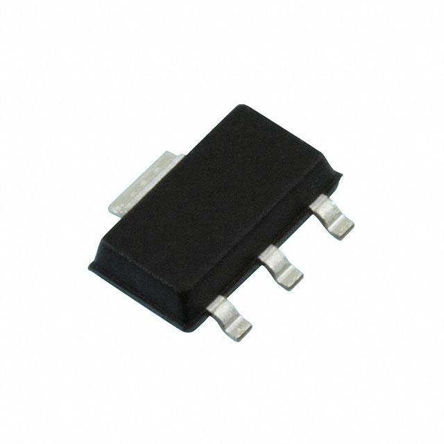
available in the very small leaded packages TO92UA-1
and TO92UA-2 and in the SMD-package SOT89B-1.
1. Introduction
1.1. Major Applications
The HAL1820 is a new member of the Micronas family
of programmable linear Hall-Effect Sensors.
The HAL1820 is a universal magnetic field sensor with
a ratiometric, linear analog output. It is produced in
CMOS technology and can be used for magnetic field
measurements, current measurements, and detection
of mechanical movement. Very accurate angle measurements or distance measurements can also be
made. The sensor is very robust and can be used in
electrically and mechanically harsh environments.
Major characteristics like magnetic field range, sensitivity, offset (output voltage at zero magnetic field) and
the temperature coefficients are programmable in a
non-volatile memory. The HAL1820 features a customer data register that enables the customer to store
production information (like production serial number)
inside each sensor.
Due to the sensor’s robust characteristics, the
HAL1820 is the optimal system solution for applications such as:
– linear position measurements,
– angle sensors,
– distance measurements,
– magnetic field and current measurement.
1.2. Features
– Ratiometric linear output proportional to the magnetic field
– Various programmable magnetic characteristics with
non-volatile memory
The sensor includes a temperature-compensated Hall
plate with choppered offset compensation, an A/D converter, digital signal processing, an EEPROM memory
with redundancy and lock function for the calibration
data, a serial interface for programming the EEPROM,
a ratiometric linear output and protection devices.
Internal digital signal processing compensates for analog offsets, temperature changes, and mechanical
stress, resulting in highly stable performance.
– Digital signal processing
The HAL1820 is programmable by modulation of the
supply voltage. No additional programming pin is
needed. The easy programmability allows a 2-point
calibration by adjusting the output signal directly to the
input signal (like mechanical angle, distance, or current). Individual adjustment of each sensor during the
customer’s manufacturing process is possible. With
this calibration procedure, the tolerances of the sensor,
the magnet and the mechanical positioning can be
compensated in the final assembly.
– Lock function and built-in redundancy for EEPROM
memory
In addition, the temperature compensation of the Hall
IC can be fit to all common magnetic materials by programming first and second order temperature coefficients of the Hall sensor sensitivity. This enables operation over the full temperature range with high
accuracy.
– operates from 4.5 V up to 5.5 V supply voltage in
specification
The calculation of the individual sensor characteristics
and the programming of the EEPROM memory can
easily be done with a PC and the application kit from
Micronas.
– Continuos measurement ranges from 20 mT to
160 mT
– Customer readable Micronas production information
(like lot number, wafer number, etc.)
– Temperature characteristics programmable for
matching all common magnetic materials
– Programming via supply voltage modulation
– Temperature and stress-stable quiescent output
voltage
– on-chip temperature compensation
– active offset compensation
– operates from 40 °C up to 170 °C
junction temperature
– operates with static magnetic fields and dynamic
magnetic fields up to 2.25 kHz
– overvoltage and reverse-voltage protection at VDD
pin
– magnetic characteristics extremely robust against
mechanical stress
– short-circuit protected push-pull output
– EMC and ESD optimized design
4
July 3, 2013; DSH000158_003EN
Micronas
�HAL 1820
DATA SHEET
1.3. Marking Code
1.6. Solderability and Welding
The HAL1820 has a marking on the package surface
(branded side). This marking includes the name of the
sensor and the temperature range.
Soldering
Type
Temperature Range
During soldering reflow processing and manual
reworking, a component body temperature of 260 °C
should not be exceeded.
A
HAL 1820
Welding
1820A
1.4. Operating Junction Temperature Range (TJ)
The Hall sensors from Micronas are specified to the
chip temperature (junction temperature TJ).
A: TJ = 40 °C to +170 °C
The relationship between ambient temperature (TA)
and junction temperature is explained in Section 4.1.
on page 22.
Device terminals should be compatible with laser and
resistance welding. Please note that the success of
the welding process is subject to different welding
parameters which will vary according to the welding
technique used. A very close control of the welding
parameters is absolutely necessary in order to reach
satisfying results. Micronas, therefore, does not give
any implied or express warranty as to the ability to
weld the component.
1.7. Pin Connections and Short Descriptions
1.5. Hall Sensor Package Codes
HALXXXPA-T
Temperature Range: A
Package: SF for SOT89B-1
UA for TO92UA-1/2
Pin No.
Pin Name
Short Description
1
VSUP
Supply Voltage and Programming Pin
2
GND
Ground
3
OUT
Push-Pull Output in
Application mode
4
GND
Ground
Type: 1820
Example: HAL1820UA-A
Type: 1820
Package: TO92UA-1/2
Temperature Range: TJ = 40 C to +170 C
1
VDD
OUT
Hall sensors are available in a wide variety of packaging versions and quantities. For more detailed information, please refer to the brochure: “Hall Sensors:
Ordering Codes, Packaging, Handling”.
3
2,4
GND
Fig. 1–1: Pin configuration
Micronas
July 3, 2013; DSH000158_003EN
5
�HAL 1820
DATA SHEET
2. Functional Description
2.1. General Function
The HAL1820 is a monolithic integrated circuit which
provides an output voltage proportional to the magnetic flux through the Hall plate and proportional to the
supply voltage (ratiometric behavior).
As long as the LOCK register is not set, the output
characteristic can be adjusted by programming the
EEPROM registers. The IC can be programmed via
VSUP line. After detecting a command, the sensor
reads or writes the memory and answers with a digital
signal on the output pin.
Output/Magnetic Field Polarity
The external magnetic field component perpendicular
to the branded side of the package generates a Hall
voltage. The Hall IC is sensitive to magnetic north and
south polarity. This voltage is converted to a digital
value, processed in the Digital Signal Processing Unit
(DSP) according to the settings of the EEPROM registers, converted back to an analog voltage by a D/A
converter and buffered by a push-pull output transistor
stage. The function and the parameter for the DSP are
explained in Section 2.2. on page 8. Internal temperature compensation circuitry and the choppered offset
compensation enables operation over the full temperature range with minimal degradation in accuracy and
offset. The circuitry also rejects offset shifts due to
mechanical stress from the package. In addition, the
sensor IC is equipped with devices for overvoltage and
reverse-voltage protection at supply pin.
A LOCK register disables the programming of the
EEPROM memory. The register can not be reset by
the customer.
Applying a south-pole magnetic field perpendicular to
the branded side of the package will increase the output voltage (for Sensitivity < 0) from the quiescent (offset) voltage towards the supply voltage. A negative
magnetic field will decrease the output voltage. The
output logic will be inverted for sensitivity >0.
In addition HAL1820 features an internal error detection. The following error modes can be detected:
– Over-/underflow in adder or multiplier
– Over-/underflow in A/D converter
– Overtemperature detection
In case of an error the sensors output will be forced to
the lower error band. The error band is defined by
VDIAG (see Section 3.6. on page 14).
VSUP
Internally
stabilized
Supply and
Protection
Devices
Switched
Hall Plate
Programming
Interface
Temperature
Dependent
Bias
Oscillator
A/D
Converter
Digital
Signal
Processing
Undervoltage
Detection
50
D/A
Converter
Analog
Output
Protection
Devices
OUT
EEPROM Memory
Lock Control
GND
Fig. 2–1: HAL1820 block diagram
6
July 3, 2013; DSH000158_003EN
Micronas
�HAL 1820
DATA SHEET
Digital Output Register
10 bit
Digital Signal Processing
Adder
A/D
Converter
TC
TCSQ
5 bit
5 bit
MRange
3 bit
Offset
8 bit
OALN
1 bit
Multiplier
Output
Sensitivity
Lock
Micronas
8 bit
1 bit
Register
Programming Parameter
Lock
Control
Fig. 2–2: Details of Programming Parameter and Digital Signal Processing
Table 2–1: Cross reference table EEPROM register and sensor parameter
EEPROM-Register
Parameter
Data Bits
Function
customer register I
Sensitivity
8
Magnetic sensitivity
Offset
8
Magnetic offset
LOCKR
1
Customer Lock
OALN
1
Magnetic Offset Alignment Bit (MSB or LSB aligned)
TCSQ
5
Quadratic temperature coefficient
TC
5
Linear temperature coefficient
MRANGE
3
Available magnetic ranges
customer register III
Micronas
Data
16
Micronas production information (read only)
customer register IV
Micronas
Data
16
Micronas production information (read only)
customer register II
Micronas
July 3, 2013; DSH000158_003EN
7
�HAL 1820
DATA SHEET
2.2. Digital Signal Processing and EEPROM
The DSP is the major part of this sensor and performs
the signal conditioning. The parameters for the DSP
are stored in the EEPROM registers. The details are
shown in Fig. 2–2.
The measurement data can be readout from the
DIGITAL OUTPUT register.
The customer can decide if the Offset is MSB aligned
or LSB aligned. The MSB or LSB alignment is enabled
by an additional Offset alignment bit (OALN). In case
the OALN bit is 1 the Offset is programmable from
50% up to 50% of VDD. This means that the Offset
covers the full-scale range. If the OALN bit is set to
zero, then the Offset covers only 1/4 of the full-scale
(12.5% up to 12.5% of VDD). The customer can
adjust the Offset symmetrically around 50% of VDD
(37.5%... 62.5% of VDD). The OFFSET register can be
set with 8-bit resolution.
DIGITAL OUTPUT
This 16-bit register delivers the actual digital value of
the applied magnetic field after the signal processing.
This register can only be read out, and it is the basis
for the calibration procedure of the sensor in the system environment. Only 10 bits of the register contain
valid data. The DIGITAL OUTPUT range is from 512
to 511.
2.2.2. Customer Register II
For Sensitivity = 1 the DIGITAL OUTPUT value will
increase for negative magnetic fields (north pole) on
the branded side of the package (positive DIGITAL
OUTPUT values).
MRANGE
Note: During application design, it should be taken
into consideration that DIGITAL OUTPUT
should not saturate in the operational range of
the specific application.
The area in the EEPROM accessible for the customer
consists of four so called customer registers with a size
of 16 bit each.
2.2.1. Customer Register I
Customer register I contains the bits for magnetic sensitivity (SENSITIVITY) and magnetic offset (OFFSET).
SENSITIVITY
Customer register II contains the bits for magnetic
range (MRANGE), linear and quadratic temperature
coefficients (TC and TCSQ), magnetic offset alignment
(OALN) and the customer lock bit.
The MRANGE bits define the magnetic field range of
the A/D converter. The following eight magnetic ranges
are available.
Table 2–2: MRANGE bit definition
Magnetic Field Range
BIT SETTING
20 mT...20 mT
0
40 mT...40 mT
1
60 mT...60 mT
2
80 mT...80 mT
3
100 mT...100 mT
4
120 mT...120 mT
5
140 mT...140 mT
6
160 mT...160 mT
7
The SENSITIVITY bits define the parameter for the
multiplier in the DSP. The Sensitivity is programmable
between 2 and 2. The SENSITIVITY bits can be
changed in steps of 0.0156. Sensitivity = 1 (@ Offset =
0) corresponds to full-scale of the output signal if the
A/D-converter value has reached the full-scale value.
OFFSET
The OFFSET bits define the parameter for the adder in
the DSP. Offset defines the output signal without external magnetic field (B = 0 mT).
8
July 3, 2013; DSH000158_003EN
Micronas
�HAL 1820
DATA SHEET
TC and TCSQ
LOCK
The temperature dependence of the magnetic sensitivity can be adapted to different magnetic materials in
order to compensate for the change of the magnetic
strength with temperature. The adaption is done by
programming the TC (Linear Temperature Coefficient)
and the TCSQ registers (Quadratic Temperature Coefficient). Thereby, the slope and the curvature of the
temperature dependence of the magnetic sensitivity
can be matched to the magnet and the sensor assembly. As a result, the output signal characteristic can be
fixed over the full temperature range. The sensor can
compensate for linear temperature coefficients ranging
from about 3100 ppm/K up to 2550 ppm/K and quadratic coefficients from about 7 ppm/K2 to 15 ppm/K2
(typical range). Min. and max. values for quadratic
temperature coefficient depend on linear temperature
coefficient. Please refer to Section 4.4. on page 22 for
the recommended settings for different linear temperature coefficients.
By setting this 1-bit register, all registers will be locked,
and the EEPROM content can not be changed anymore. It is still possible to read all register content by
sending a read command to the sensor. The LOCK bit
is active after the first power-off and power-on
sequence after setting the LOCK bit.
Warning: This register cannot be reset!
2.2.3. Customer register III and IV
Customer register III and IV contain 16 bits each.
These two registers can be read by the customer and
Micronas will use this register to store production information like wafer position, wafer number and production lot number.
Magnetic Offset Alignment Bit (OALN)
Please refer to Section 2.2.1. on page 8 (OFFSET).
Micronas
July 3, 2013; DSH000158_003EN
9
�HAL 1820
DATA SHEET
ADC
+FS
{
+range
0
FS
{
range
}
8-bit offset value (128...+127) 8-bit sensitivity value (128...+127)
±1
x
±2
±0.5 (OALN = 0)
±0.125 (OALN = 1)
+
ADC value
range ±7936
FS ~
~ range
10-bit readout-value (512...+511)
*
clamp
y/n
y
±1 @ offset = 0 and sensitivity = 1
adder out
range 8192/8191
Definition: FS of ADC = 1.
Fig. 2–3: Signal path HAL1820
2.2.4. Signal Path
Locking the Sensor
Fig. 2–3 shows the signal path and signal processing
of HAL1820. The measurement output value y is calculated out of the input signal X with the following
equation
The last step is activating the LOCK function by setting
the LOCK bit. Please note that the LOCK function
becomes effective after power-down and power-up of
the Hall IC. The sensors EEPROM is then locked and
its content can not be changed anymore. The sensor
still answers to read commands on the supply line.
Y = sensitivity X – OFFSET
The parameters offset and sensitivity are two’s complement encoded 8-bit values (see Section 2.2.1. on
page 8).
Warning: This register cannot be reset!
2.3. Calibration Procedure
2.3.1. General Procedure
For calibration in the system environment, the application kit from Micronas is recommended. It contains the
hardware for the generation of the serial telegram for
programming and the corresponding software for the
input of the register values.
For the individual calibration of each sensor in the customer application, a two-point adjustment is recommended. Please use Micronas Software Kit for the calibration.
10
July 3, 2013; DSH000158_003EN
Micronas
�HAL 1820
DATA SHEET
3. Specifications
3.1. Outline Dimensions
Fig. 3–1:
SOT89B-1: Plastic Small Outline Transistor package, 4 leads
Ordering code: SF
Weight approximately 0.034 g
Micronas
July 3, 2013; DSH000158_003EN
11
�HAL 1820
DATA SHEET
A2
A3
E1
A4
Bd
F1
D1
y
Center of sensitive area
F3
F2
3
L1
2
L
1
e
c
4
b
physical dimensions do not include moldflash.
0
5 mm
2.5
solderability is guaranteed between end of pin and distance F1.
scale
Sn-thickness might be reduced by mechanical handling.
A4, y= these dimensions are different for each sensor type and is specified in the data sheet.
min/max of D1 are specified in the datasheet.
UNIT
A2
A3
b
Bd
c
D1
e
E1
F1
F2
F3
L
L1
4
mm
1.55
1.45
0.7
0.42
0.2
0.36
3.05
2.54
4.11
4.01
1.2
0.8
0.60
0.42
4.0
2.0
15.5
min
15.0
min
45°
JEDEC STANDARD
ANSI
ISSUE
ITEM NO.
-
-
ISSUE DATE
YY-MM-DD
DRAWING-NO.
ZG-NO.
09-06-09
06616.0001.4
ZG001016_Ver.06
Fig. 3–2:
TO92UA-1: Plastic Transistor Standard UA package, 3 leads, spread
Weight approximately 0.106 g
12
July 3, 2013; DSH000158_003EN
Micronas
�HAL 1820
DATA SHEET
A2
A3
E1
A4
Bd
F1
D1
y
Center of sensitive area
1
2
3
L
F2
e
b
4
c
physical dimensions do not include moldflash.
0
2.5
solderability is guaranteed between end of pin and distance F1.
5 mm
scale
Sn-thickness might be reduced by mechanical handling.
A4, y= these dimensions are different for each sensor type and is specified in the data sheet.
min/max of D1 are specified in the datasheet.
UNIT
A2
A3
b
Bd
c
D1
e
E1
F1
F2
L
4
mm
1.55
1.45
0.7
0.42
0.2
0.36
3.05
1.27
4.11
4.01
1.2
0.8
0.60
0.42
15.5
min
45°
JEDEC STANDARD
ANSI
ISSUE
ITEM NO.
-
-
ISSUE DATE
YY-MM-DD
DRAWING-NO.
ZG-NO.
09-06-05
06612.0001.4
ZG001012_Ver.07
Fig. 3–3:
TO92UA-2: Plastic Transistor Standard UA package, 3 leads, not spread
Weight approximately 0.106 g
Micronas
July 3, 2013; DSH000158_003EN
13
�HAL 1820
DATA SHEET
Fig. 3–4:
TO92UA/UT-1: Dimensions ammopack inline, spread
14
July 3, 2013; DSH000158_003EN
Micronas
�HAL 1820
DATA SHEET
Fig. 3–5:
TO92UA/UT-2: Dimensions ammopack inline, not spread
Micronas
July 3, 2013; DSH000158_003EN
15
�HAL 1820
DATA SHEET
3.2. Dimensions of Sensitive Area
0.2 mm x 0.1 mm
3.3. Package Dimensions
TO92UA-1/-2
SOT89B-1
y
1.0 mm nominal
0.95 mm nominal
A4
0.4 mm nominal
0.4 mm nominal
D1
3.05 0.05 mm
2.55 0.05 mm
H1
min. 21 mm
max. 23.1 mm
not applicable
3.4. Absolute Maximum Ratings
Stresses beyond those listed in the “Absolute Maximum Ratings” may cause permanent damage to the device. This
is a stress rating only. Functional operation of the device at these conditions is not implied. Exposure to absolute
maximum rating conditions for extended periods will affect device reliability.
This device contains circuitry to protect the inputs and outputs against damage due to high static voltages or electric
fields; however, it is advised that normal precautions be taken to avoid application of any voltage higher than absolute maximum-rated voltages to this circuit.
All voltages listed are referenced to ground (GND).
Symbol
Parameter
Pin No.
Min.
Max.
Unit
Condition
VSUP
Supply Voltage
1
8.5
14.4
15
8.5
14.4
16
V
t < 96 h
t < 10 min.
t < 1 min.
not additive
VOUT
Output Voltage
3
0.51)
0.51)
0.51)
8.5
14.4
16
V
t < 96 h
t < 10 min.
t < 1 min.
not additive
VOUT VSUP
Excess of Output Voltage
over Supply Voltage
1,3
0.5
V
IOUT
Continuous Output Current
3
5
5
mA
tSh
Output Short Circuit Duration
3
10
min
TJ
Junction Temperature under
Bias
40
190
°C
VESD
ESD Protection3)
4.0
4.0
kV
1)
internal protection resistor = 50
2)
for 96h - Please contact Micronas for
3) AEC-Q100-002 (100 pF and 1.5 k
16
1,2,3
2)
other temperature requirements
July 3, 2013; DSH000158_003EN
Micronas
�HAL 1820
DATA SHEET
3.4.1. Storage and Shelf Life
The permissible storage time (shelf life) of the sensors is unlimited, provided the sensors are stored at a maximum of
30 °C and a maximum of 85% relative humidity. At these conditions, no Dry Pack is required.
Solderability is guaranteed for one year from the date code on the package.
3.5. Recommended Operating Conditions
Functional operation of the device beyond those indicated in the “Recommended Operating Conditions/Characteristics” is not implied and may result in unpredictable behavior of the device and may reduce reliability and lifetime.
All voltages listed are referenced to ground (GND).
Symbol
Parameter
Pin No.
Min.
Typ.
Max.
Unit
Remarks
VSUP
Supply Voltage
1
4.5
5.7
5
5.85
5.5
6.0
V
Normal operation
During programming
IOUT
Continuous Output Current
3
1
1
mA
RL
Load Resistor
3
5.5
10
k
CL
Load Capacitance
3
0.33
10
47
nF
NPRG
Number of EEPROM
Programming Cycles
100
0 °C < Tamb < 55 °C
TJ
Junction Operating
Temperature1)
40
40
40
125
150
170
°C
°C
°C
for 8000 hrs
for 2000 hrs
for 1000 hrs
Time values are not additive.
1)
Depends on the temperature profile of the application. Please contact Micronas for life time calculations.
Micronas
July 3, 2013; DSH000158_003EN
17
�HAL 1820
DATA SHEET
3.6. Characteristics
at TJ = 40 °C to +170 °C (for temperature type A), VSUP = 4.5 V to 5.5 V, GND = 0 V, after programming the sensor
and locking the EEPROM,
at Recommended Operation Conditions if not otherwise specified in the column “Conditions”.
Typical Characteristics for TJ = 25 °C and VSUP = 5 V.
Symbol
Parameter
Pin No.
Min.
Typ.
Max.
Unit
Conditions
ISUP
Supply Current
over Temperature Range
1
7
10
mA
Resolution
3
10
Bit
INL
Non-Linearity of Output
Voltage over Temperature
3
1.0
0
1.0
%
ER
Ratiometric Error of Output
over Temperature
(Error in VOUT / VSUP)
3
1.0
0
1.0
%
VOUTH
Output High Voltage
3
4.7
4.9
V
VSUP = 5 V, IOUT = +/ 1 mA2)
VOUTL
Output Low Voltage
3
0.1
0.3
V
VSUP = 5 V, IOUT = +/ 1 mA2)
tr(O)
Response Time of Output3)
3
0.5
1
ms
CL = 10 nF, time from 10% to
90% of final output voltage for a
step like
signal Bstep from 0 mT to Bmax
tPOD
Power-Up Time (Time to
reach stabilized Output
Voltage)3)
1
1.5
ms
CL = 10 nF, 90% of VOUT
BW
Small Signal Bandwidth (
3 dB)3)
3
2.25
2.5
kHz
BAC < 10 mT
VOUTn
Output RMS Noise3)
3
2.6
5
mV
B = 5% to 95% of Bmax
ROUT
Output Resistance over
Recommended Operating
Range3)
3
60
VOUTLmax VOUT VOUTHmin
VPORLH
Power-On Reset Level from
VSUPLow to VSUPHigh
1
3.9
4.35
4.5
V
VPORHL
Power-On Reset Level from
VSUPHighto VSUPLow
1
3.8
4.2
4.4
V
VPORHYS
Power-On Reset Hysteresis
1
0.1
0.175
0.3
V
VDIAG
Output Voltage in case of
Error Detection
3
0
300
mV
% of supply voltage1)
TO92UA Package
Thermal Resistance
Measured with a 1s0p board
Rthja
junction to air
250
K/W
Rthjc
junction to case
70
K/W
SOT89B Package
Thermal Resistance
Rthja
junction to air
210
K/W
Rthjc
junction to case
60
K/W
Measured with a 1s0p board
30 mm x 10 mm x 1.5 mm,
pad size (see Fig. 3–6)
1)
If more than 50% of the selected magnetic field range are used and VOUT is between 0.3 V and 4.7 V
2)
Linear output range
3)
Guaranteed by design
18
July 3, 2013; DSH000158_003EN
Micronas
�HAL 1820
DATA SHEET
1.80
1.05
1.45
2.90
1.05
0.50
1.50
Fig. 3–6: Recommended footprint SOT89B-1, Dimensions in mm.
All dimensions are for reference only. The pad size may vary depending on the requirements of the soldering
process.
3.7. Magnetic Characteristics
at Recommended Operating Conditions if not otherwise specified in the column ’Test Conditions’,
TJ =40 °C to +170 °C (for temperature type A), VSUP = 4.5 V to 5.5 V, after programming the sensor and locking the
EEPROM.
Typical Characteristics for TA = 25 °C and VSUP = 5 V.
Symbol
Parameter
RANGEABS Absolute Magnetic Range
of A/D Converter over
temperature
RANGE
Magnetic field range
Values
Pin No.
Min.
Typ.
Max.
80
100
120
20
110
10
Senstrim
Trim step for absolute
sensitivity1)
3
0.3
Offset trim1)
3
Micronas
160
160
3
Sensitivity Error over Temperature Range
80
40
Trim range for absolute
sensitivity1)
ES
Test Conditions
%
% of nominal RANGE
Nominal RANGE programmable from
20 mT up to 160 mT
Sensitivity
Offsettrim
Unit
1
3
2.5
312
10
1250
6
0
July 3, 2013; DSH000158_003EN
6
mT
TO92UA-1/-2
SOT89B-1
mV/
mT
Depending on magnetic field range 1) and
SENS register content
mV/
mT
At min. sensitivity
mV
OALN=0
At max. sensitivity
OALN=1
%
Part to part variation
for certain combinations of TC and TCSQ
(see Section 3.7.1.)
19
�HAL 1820
Symbol
DATA SHEET
Parameter
Values
Pin No.
Unit
Test Conditions
Min.
Typ.
Max.
2
%
TJ = 25 °C; after temperature cycling and
over life time
SensLife
Sensitivity Drift (beside
temperature drift)1)
BOFFSET
Magnetic offset
3
2
0
2
mT
B = 0 mT, TA = 25 °C
BOFFSET
Magnetic offset drift over
Temperature Range
3
300
0
300
µT
B = 0 mT, RANGE =
20 mT, Sens = 100
mV/mT
3
20
0
20
µT
Range = 40 mT
BOFFSET(T) BOFFSET
(25 °C)
BHysteresis
1)
Magnetic Hysteresis1)
Guaranteed by design
ideal 200 ppm/k
1.03
relative sensitivity related to 25 °C value
least-square-fit straight-line of
normalized measured data
measurement example of real
sensor, normalized to achieve a
value of 1 of its least-square-fit
straight-line at 25 °C
1.02
1.01
1.001
1.00
0.993
0.99
0.98
-50
-25
-10
0
25
50
75 100
temperature [°C]
125
150
175
Fig. 3–7: Definition of Sensitivity Error ES.
20
July 3, 2013; DSH000158_003EN
Micronas
�HAL 1820
DATA SHEET
3.7.1. Definition of Sensitivity Error ES
ES is the maximum of the absolute value of 1 minus
the quotient of the normalized measured value1) over
the normalized ideal linear2) value:
ES = max abs meas
------------ – 1
ideal
In the example shown in Fig. 3–7 the maximum error
occurs at 10 °C:
ES = 1.001
------------- – 1 = 0.8%
0.993
Tmin, Tmax
1) normalized to achieve a least-square-fit straight-line
that has a value of 1 at 25 °C
2) normalized to achieve a value of 1 at 25 °C
Micronas
July 3, 2013; DSH000158_003EN
21
�HAL 1820
DATA SHEET
4. Application Notes
VSUP
4.1. Ambient Temperature
Due to the internal power dissipation, the temperature
on the silicon chip (junction temperature TJ) is higher
than the temperature outside the package (ambient
temperature TA).
OUT
HAL1820
100 nF
TJ = TA + T
47 nF
GND
At static conditions and continuous operation, the following equation applies:
Fig. 4–1: Recommended application circuit
T = ISUP * VSUP * RthjX
The X represents junction to air or to case.
4.4. Temperature Compensation
For worst case calculation, use the max. parameters
for ISUP and RthjX, and the max. value for VSUP from
the application.
The relationship between the temperature coefficient
of the magnet and the corresponding TC and TCSQ
codes for linear compensation is given in the following
table. In addition to the linear change of the magnetic
field with temperature, the curvature can be adjusted
as well. For this purpose, other TC and TCSQ combinations are required which are not shown in the table.
Please contact Micronas for more detailed information
on this higher order temperature compensation.
The following example shows the result for junction to
air conditions. VSUP = 5.5 V, Rthja = 250 K/W and ISUP
= 10 mA the temperature difference T = 13.75 K.
The junction temperature TJ is specified. The maximum ambient temperature TAmax can be calculated as:
TAmax = TJmax T
Temperature Coefficient
of Magnet (ppm/K)
4.2. EMC and ESD
The HAL1820 is designed for a stabilized 5 V supply.
Interferences and disturbances conducted along the
12 V onboard system (product standard ISO 7637 part
1) are not relevant for these applications.
For applications with disturbances by capacitive or
inductive coupling on the supply line or radiated disturbances, the application circuit shown in Fig. 4–1 is recommended. Applications with this arrangement should
pass the EMC tests according to the product standards ISO 7637 part 3 (Electrical transient transmission by capacitive or inductive coupling) and part 4
(Radiated disturbances).
4.3. Application Circuit
For EMC protection, it is recommended to connect one
ceramic 47 nF capacitor between ground and output
voltage pin as well as 100 nF between supply and
ground.
TC
TCSQ
2100
8
0
1800
10
3
1500
12
4
1200
14
5
900
16
6
500
18
6
150
20
6
0
21
5
300
22
5
500
23
4
750
24
4
1000
25
2
1500
27
0
2100
29
5
2700
31
5
Note: Micronas recommends to use the HAL1820
Programming Environment to find optimal settings for temperature coefficients. Please contact Micronas for more detailed information.
22
July 3, 2013; DSH000158_003EN
Micronas
�HAL 1820
DATA SHEET
5. Programming of the Sensor
HAL1820 features two different customer modes. In
Application Mode the sensor provides a ratiometric
analog output voltage. In Programming Mode it is
possible to change the register settings of the sensor.
The serial telegram is used to transmit the EEPROM
content, error codes and digital values of the magnetic
field from and to the sensor.
tr
tf
VDDH
After power-up the sensor is always operating in the
Programming Mode (default after delivery from
Micronas and as long as the sensor is not locked). It is
switched to the Application Mode by setting a certain
volatile bit in the memory of the sensor or by locking
the sensor.
tp0
logical 0
VDDL
tp1
VDDH
tp0
logical 1
5.1. Programming Interface
In Programming Mode the sensor is addressed by
modulating a serial telegram on the sensors supply
voltage. The sensor answers with a modulation of the
output voltage.
A logical “0” is coded as no level change within the bit
time. A logical “1” is coded as a level change of typically 50% of the bit time. After each bit, a level change
occurs (see Fig. 5–1).
tp0
or
VDDL
or
tp0
tp1
Fig. 5–1: Definition of logical 0 and 1 bit
A description of the communication protocol and the
programming of the sensor is available in a separate
document (Application Note Programming HAL1820).
Table 5–1: Telegram parameters (All voltages are referenced to GND.)
Symbol
Parameter
Pin No.
Limit Values
Unit
Min.
Typ.
Max.
VSUPL
Supply Voltage for Low Level
during Programming through
Sensor VSUP Pin
1
5.8
6.3
6.6
V
VSUPH
Supply Voltage for High Level
during Programming through
Sensor VSUP Pin
1
6.8
7.3
7.8
V
VSUPProgram
VSUP Voltage for EEPROM
programming (after PROG and
ERASE)
1
5.7
5.85
6.0
V
tp0
Bit time if command send to the
sensor
1
1024
µs
tpOUT
Bit time for sensor answer
3
1024
µs
Micronas
July 3, 2013; DSH000158_003EN
Test Conditions
23
�HAL 1820
DATA SHEET
5.2. Programming Environment and Tools
For the programming of HAL1820 during product
development and also for production purposes a programming tool including hardware and software is
available on request. It is recommended to use the
Micronas tool kit in order to easy the product development. The details of programming sequences are also
available on request.
5.3. Programming Information
For production and qualification tests, it is mandatory
to set the LOCK bit after final adjustment and programming of HAL1820. The LOCK function is active after
the next power-up of the sensor.
The success of the LOCK process should be checked
by reading the status of the LOCK bit after locking and/
or by an analog check of the sensors output signal.
HAL1820 features a diagnostic register to check the
success and quality of the programming process. It is
mandatory to check that all bits of the DIAGN register
are 0 after the programming of the sensor. More
details can be found in the application note “HAL1820
Programming Guide”.
Electrostatic Discharges (ESD) may disturb the programming pulses. Please take precautions against
ESD.
24
July 3, 2013; DSH000158_003EN
Micronas
�HAL 1820
DATA SHEET
6. Data Sheet History
1. Advance Information: “HAL 1820, Programmable
Linear Hall-Effect Sensor”, June 30, 2009,
AI000149_001EN. First release of the advance
information.
2. Advance Information: “HAL 1820, Programmable
Linear Hall-Effect Sensor”, April 28, 2010,
AI000149_002. Second release of the advance
information.
Major Changes:
– Reset levels added
– TC/TCSQ table added
– Update of magnetic parameters
3. Data Sheet: “HAL 1820 Programmable Linear HallEffect Sensor”, April 28, 2011, DSH000158_001EN.
First release of the data sheet.
4. Data Sheet: “HAL 1820 Programmable Linear HallEffect Sensor”, April 23, 2013, DSH000158_002EN.
Second release of the data sheet.
Major Changes:
– Temperature range “K” removed
5. Data Sheet: “HAL 1820 Programmable Linear HallEffect Sensor”, July 3, 2013, DSH000158_003EN.
Third release of the data sheet.
Major Changes:
– Section 3.7. Magnetic Characteristics
Micronas GmbH
Hans-Bunte-Strasse 19 D-79108 Freiburg P.O. Box 840 D-79008 Freiburg, Germany
Tel. +49-761-517-0 Fax +49-761-517-2174 E-mail: docservice@micronas.com Internet: www.micronas.com
25
July 3, 2013; DSH000158_003EN
Micronas
�