HAL1880UA-A-2-A-2-00 数据手册
Hardware
Documentation
D at a S h e e t
®
HAL 1880
Programmable Linear Hall-Effect
Sensor in TO92 Package
Edition Sept. 8, 2020
DSH000198_003EN
�HAL 1880
DATA SHEET
Copyright, Warranty, and Limitation of Liability
The information and data contained in this document are believed to be accurate and reliable. The software and proprietary information contained therein may be protected by
copyright, patent, trademark and/or other intellectual property rights of TDK-Micronas. All
rights not expressly granted remain reserved by TDK-Micronas.
TDK-Micronas assumes no liability for errors and gives no warranty representation or
guarantee regarding the suitability of its products for any particular purpose due to
these specifications.
By this publication, TDK-Micronas does not assume responsibility for patent infringements
or other rights of third parties which may result from its use. Commercial conditions, product availability and delivery are exclusively subject to the respective order confirmation.
Any information and data which may be provided in the document can and do vary in
different applications, and actual performance may vary over time.
All operating parameters must be validated for each customer application by customers’
technical experts. Any mention of target applications for our products is made without a
claim for fit for purpose as this has to be checked at system level.
Any new issue of this document invalidates previous issues. TDK-Micronas reserves
the right to review this document and to make changes to the document’s content at any
time without obligation to notify any person or entity of such revision or changes. For
further advice please contact us directly.
Do not use our products in life-supporting systems, military, aviation, or aerospace
applications! Unless explicitly agreed to otherwise in writing between the parties,
TDK-Micronas’ products are not designed, intended or authorized for use as components in systems intended for surgical implants into the body, or other applications
intended to support or sustain life, or for any other application in which the failure of the
product could create a situation where personal injury or death could occur.
No part of this publication may be reproduced, photocopied, stored on a retrieval system or transmitted without the express written consent of TDK-Micronas.
TDK-Micronas Trademarks
– HAL
Third-Party Trademarks
All other brand and product names or company names may be trademarks of their
respective companies.
TDK-Micronas GmbH
Sept. 8, 2020; DSH000198_003EN
2
�HAL 1880
DATA SHEET
Contents
Page
Section
Title
4
5
5
1.
1.1.
1.2.
Introduction
Major Applications
Features
6
6
2.
2.1.
Ordering Information
Device-Specific Ordering Codes
7
7
8
9
9
10
10
12
13
14
15
15
15
3.
3.1.
3.2.
3.2.1.
3.2.2.
3.2.3.
3.2.4.
3.2.5.
3.2.6.
3.3.
3.4.
3.4.1.
3.4.2.
Functional Description
General Function
Digital Signal Processing and EEPROM
Digital Output Register
Output Scaling Register
Micronas ID Number Registers
Customer Setup 1 Registers
Customer Setup 2 Register
Signal Path
On-Board Diagnostic Features
Sensor Calibration
General Procedure for Development or Evaluation Purposes
Locking the Sensor
16
16
20
20
20
20
21
22
22
23
26
27
27
28
29
4.
4.1.
4.2.
4.3.
4.4.
4.5.
4.6.
4.7.
4.8.
4.9.
4.9.1.
4.10.
4.11.
4.12.
4.12.1.
Specifications
Outline Dimensions
Soldering, Welding and Assembly
Pin Connections and Short Descriptions
Dimensions of Sensitive Area
Output/Magnetic-Field Polarity
Absolute Maximum Ratings
Storage and Shelf Life
Recommended Operating Conditions
Characteristics
Definition of tPOD
Power-On Reset / Undervoltage Detection
Output Voltage in Case of Error Detection
Magnetic Characteristics
Definition of Sensitivity Error ES
30
30
30
31
32
5.
5.1.
5.2.
5.3.
5.4.
Application Notes
Ambient Temperature
EMC
Application Circuit
Temperature Compensation
33
33
34
34
6.
6.1.
6.2.
6.3.
Programming of the Sensor
Programming Interface
Programming Environment and Tools
Programming Information
35
7.
Document History
TDK-Micronas GmbH
Sept. 8, 2020; DSH000198_003EN
3
�HAL 1880
DATA SHEET
Release Note:
Revision bars indicate significant changes to the previous edition.
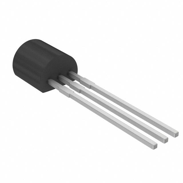
Programmable Linear Hall-Effect Sensor in TO92 Package
1. Introduction
The HAL 1880 is a universal programmable Hall-effect sensor with a ratiometric, linear
analog output proportional to the magnetic flux density applied to the sensor surface.
The sensor can be used for magnetic-field measurements such as current measurements and detection of mechanical movement, like for small-angle or distance measurements. The sensor is robust and can be used in harsh electrical and mechanical
environments.
Major characteristics like magnetic-field range, sensitivity, offset (output voltage at zero
magnetic field) and the temperature coefficients are programmable in a non-volatile
memory. Several output signal clamping levels can be programmed. Diagnostic features are implemented to indicate various fault conditions like undervoltage, under-/
overflow or overtemperature.
The HAL 1880 is programmable by modulating the supply voltage with a serial telegram on
the sensor’s output pin or supply pin. No additional programming pin is needed. Several
sensors on the same supply line can be programmed individually (communication through
OUT pins). This programmability allows a 2-point calibration by adjusting the output signal
directly to the input signal, such as mechanical angle, distance or current.
Individual adjustment of each sensor during the customer’s manufacturing process is
possible. With this calibration procedure, the tolerance of the sensor, the magnet and
the mechanical positioning can be compensated in the final assembly.
The spinning-current offset compensation leads to stable magnetic characteristics over
supply voltage and temperature. Furthermore, the first and seconds order temperature
coefficients of the sensor sensitivity can be used to compensate the temperature drift of
all common magnetic materials. This enables operation over the full temperature range
with high accuracy.
The calculation of the individual sensor characteristics and the programming of the
EEPROM memory can easily be done with a PC and the application kit from
TDK-Micronas.
The sensor is designed for industrial and automotive applications, is AEC-Q100 qualified, and operates in the junction temperature range from –40 °C up to 170 °C. The
HAL 1880 is available in the very small leaded package TO92UA-1 and TO92UA-2.
TDK-Micronas GmbH
Sept. 8, 2020; DSH000198_003EN
4
�HAL 1880
DATA SHEET
1.1. Major Applications
Thanks to the sensor's robust and cost-effective design, the HAL 1880 is the optimal
system solution for applications such as:
– Small-angle or linear position measurements
– Gear position detection in transmission application
– Current sensing for battery management
– Rotary selector
1.2. Features
– Ratiometric linear output proportional to the magnetic field
– Digital signal processing
– Continuous measurement ranges from 20 mT to 160 mT
– Selectable clamping levels with selectable diagnosis
– Comprehensive diagnostic feature set
– Lock function and built-in redundancy for EEPROM memory
– Programmable temperature characteristics for matching all common magnetic materials
– Programming via output pin or supply voltage modulation
– On-chip temperature compensation
– Active offset compensation
– Operates from 40 °C up to 170 °C junction temperature
– Operates from 4.5 V up to 5.5 V supply voltage in specification
– Operates with static and dynamic magnetic fields up to 5 kHz
– Selectable sampling frequency (8 kHz or 16 kHz)
– Overvoltage and reverse-voltage protection at VSUP pin
– Magnetic characteristics extremely robust against mechanical stress
– Short-circuit protected push-pull output
– EMC and ESD optimized design
– AEC-Q100 qualified
TDK-Micronas GmbH
Sept. 8, 2020; DSH000198_003EN
5
�HAL 1880
DATA SHEET
2. Ordering Information
A Micronas device is available in a variety of delivery forms. They are distinguished by a
specific ordering code:
XXX NNNN PA-T-C-P-Q-SP
Further Code Elements
Temperature Range
Package
Product Type
Product Group
Fig. 2–1: Ordering code principle
For a detailed information, please refer to the brochure: “Sensors and Controllers:
Ordering Codes, Packaging, Handling”.
2.1. Device-Specific Ordering Codes
HAL 1880 is available in the following package and temperature variants.
Table 2–1: Available packages
Package Code (PA)
Package Type
UA
TO92UA
Table 2–2: Available temperature ranges
Temperature Code (T)
Temperature Range
A
TJ = 40 °C to 170 °C
The relationship between ambient temperature (TA) and junction temperature (TJ) is
explained in Section 5.1. on page 30.
For available variants for Configuration (C), Packaging (P), Quantity (Q), and Special
Procedure (SP) please contact TDK-Micronas.
Table 2–3: Available ordering codes and corresponding package marking
Available Ordering Codes
Package Marking
HAL 1880UA-A-[C-P-Q-SP]
1880A
TDK-Micronas GmbH
Sept. 8, 2020; DSH000198_003EN
6
�HAL 1880
DATA SHEET
3. Functional Description
3.1. General Function
The HAL1880 is a monolithic integrated circuit (IC) which provides an output voltage
proportional to the magnetic flux through the Hall plate and proportional to the supply
voltage (ratiometric behavior).
The Hall IC is sensitive to magnetic north and south polarity. This Hall voltage is converted
to a digital value, processed in the Digital Signal Processing unit (DSP) according to the
settings of the EEPROM registers, converted back to an analog voltage by a D/A converter
(DAC) and buffered by a push-pull output stage. Selectable clamping levels for the output
voltage as well as diagnostic features are available. The function and the parameter for the
DSP are explained in Section 3.2. on page 8. Internal temperature compensation circuitry
and spinning-current offset compensation enable operation over the full temperature range
with minimal degradation in accuracy and offset. The circuitry also rejects offset shifts due
to mechanical stress from the package. In addition, the sensor IC is equipped with devices
for overvoltage and reverse polarity protection at supply pin.
VSUP
Internally
stabilized
Supply and
Protection
Devices
Switched
Hall Plate
Programming
Interface
Temperature
Dependent
Bias
A/D
Converter
Oscillator
Digital
Signal
Processing
Overtemperature
Detection
Undervoltage
Detection
Protection
Devices
50
Clamping
D/A
Converter
Analog
Output
OUT
EEPROM Memory
Diagnosis
Lock Control
GND
Fig. 3–1: HAL1880 block diagram
The IC can be programmed via supply or output pin voltage modulation. After detecting
a command, the sensor reads or writes the memory and answers with a digital signal on
the output pin. As long as the LOCK register is not set, the output characteristic can be
adjusted by programming the EEPROM registers. The LOCK register disables the programming of the EEPROM memory. This register cannot be reset.
Furthermore, HAL1880 features an internal error detection. The following error modes
can be detected: over-/underflow in adder or multiplier, over-/underflow in A/D converter
(ADC) and overtemperature.
TDK-Micronas GmbH
Sept. 8, 2020; DSH000198_003EN
7
�HAL 1880
DATA SHEET
3.2. Digital Signal Processing and EEPROM
Hall Plate
DIAGNO SIS
DSP
M ultiplier
Clamping
DSDO U BLE
M AG_RANGE
SENSITIV ITY
CLAM P_SP
CLEV EL
M DATA
Adder
O FFSET
O FFSET_ALIGN
A/ D Converter
TC
TCSQ
O utput Controller
D/ A
Converter
V OUT
EN_ERC_HI
CLAM P_ERC
Customer Programmable Parameters
Fig. 3–2: Details of Programming Parameter and Digital Signal Processing
Table 3–1: Cross reference table for EEPROM register and sensor parameter
EEPROM-Register
Parameter
Data
Bits
Function
Customer Setup 1
DSDOUBLE
1
Sampling frequency
CLEVEL
2
Output clamping values selection
EN_ERC_HI
1
Enables High and Low error band
TC_FINE
1
Fine adjustment of linear temperature coefficient
LOCK
1
Customer lock
CLAMP_SP
1
Activates unbalanced clamping levels
OFFSET_
ALIGN
1
Magnetic offset alignment bit (MSB or LSB
aligned)
TCSQ
5
Quadratic temperature coefficient
TC
5
Linear temperature coefficient
MAG_RANGE
3
Available magnetic ranges
SENSITIVITY
8
Magnetic sensitivity
OFFSET
8
Magnetic offset
Micronas ID1
MIC_ID_1
16
Micronas production information (read only)
Micronas ID2
MIC_ID_2
16
Micronas production information (read only)
Customer Setup 2
Output Scaling
Note
For more information on the registers and the memory map of the HAL1880,
please refer to the application note “HAL1880/HAL 1890 User Manual”.
TDK-Micronas GmbH
Sept. 8, 2020; DSH000198_003EN
8
�HAL 1880
DATA SHEET
The DSP is a key function of this sensor and performs the signal conditioning. The
parameters for the DSP are stored in the EEPROM registers. Details are shown in
Fig. 3–2 on page 8.
The measurement data can be readout from the digital output register MDATA.
3.2.1. Digital Output Register
MDATA register
This 16-bit register delivers the actual digital value of the applied magnetic field after the
signal processing. This register can only be read out, and it is the basis for the calibration procedure of the sensor in the customer application. Only 10 bits of the register
contain valid data. The MDATA range is from 512 to 511.
The area in the EEPROM accessible to the customer consists of registers with a size of
16 bits each.
For SENSITIVITY = 1 the MDATA value will increase for negative magnetic fields (north
pole) on the branded side of the package (positive MDATA values).
Note
During application design, it shall be taken into consideration that the
MDATA value should not saturate in the full operational range of the specific
application.
3.2.2. Output Scaling Register
The Output Scaling register contains the bits for magnetic sensitivity (SENSITIVITY)
and magnetic offset (OFFSET).
SENSITIVITY
The SENSITIVITY bits define the parameter for the multiplier in the DSP and is programmable between [2...2] in steps of 0.0156. SENSITIVITY = 1 (at Offset = 0) corresponds
to full-scale (FS) of the output signal if the A/D converter value has reached the full-scale
value. The SENSITIVITY register has a resolution of 8 bits.
OFFSET
The OFFSET bits define the parameter for the adder in the DSP.
The customer can decide if the offset is MSB aligned or LSB aligned. The MSB or LSB
alignment is enabled by an additional offset alignment bit (OFFSET_ALIGN). In case this
bit is set to 1, the offset is programmable from 25% up to 25% of VSUP. If the
OFFSET_ALIGN bit is set to zero, then the offset covers only 1/8 of the full-scale (6.25%
up to 6.25% of VSUP) but with finer step size. The customer can adjust the offset
symmetrically around 50% of VSUP. The OFFSET register can be set with 8-bit resolution.
TDK-Micronas GmbH
Sept. 8, 2020; DSH000198_003EN
9
�HAL 1880
DATA SHEET
3.2.3. Micronas ID Number Registers
Micronas ID Number registers contain 16 bits each. TDK-Micronas will use the registers
to store production information like wafer position, wafer number and production lot
number. These two registers can be read by the customer.
3.2.4. Customer Setup 1 Registers
The Customer Setup 1 register contains the bits to select the sampling frequency, to
enable/disable the High Error Band for error indication, and to define the output signal
clamping levels.
DSDOUBLE
The bit DSDOUBLE allows to double the sampling frequency. The permitted values are
8 kHz and 16 kHz, corresponding to a bandwidth of 2.5 kHz and 5 kHz.
CLEVEL
The 2-bit CLEVEL together with CLAMP_SP select the clamping levels, i.e. the maximum and minimum output voltage levels of the analog output. The following choices are
available {CLAMP_SP:CLEVEL}:
Table 3–2: Clamping level definition
CLAMP_SP
CLEVEL
Clamping Level (%VSUP)
low
high
0
00
VOUTL
VOUTH
0
01
5
95
0
10
10
90
0
11
15
85
1
00
5
90
1
01
10
95
1
10
20
90
1
11
10
80
TDK-Micronas GmbH
Sept. 8, 2020; DSH000198_003EN
10
�HAL 1880
DATA SHEET
Clamping is normally not considered as an error. However, the user is able to activate
the clamping error code by setting the CLAMP_ERC bit of the Customer Setup 1 register.
In that case the output will be forced to the Low Error Band (VDIAG_L) or High Error
Band (VDIAG_H), as soon as the output signal reaches the programmed clamping levels.
The upper error band is realized by setting the MDATA register to maximum value. The
resulting clamping behavior therefore depends on the selection of the clamping levels,
the setting of the CLAMP_ERC bit, and the setting of the EN_ERC_HI bit (Error Code
Selection). All possible clamping variations are shown in Fig. 3–3.
Output Voltage
VDIAG_H
High Error Band
High
Clamping Level
No Clamping Levels selected
Clamping Levels selected:
CLAMP_ERC = 0
CLAMP_ERC = 1 & DIS_ER_LOW = 0
CLAMP_ERC = 1 & DIS_ER_LOW = 1
Low
Clamping Level
VDIAG_L
Low Error Band
Magnetic Field Amplitude
Fig. 3–3: HAL1880 clamping behavior
TDK-Micronas GmbH
Sept. 8, 2020; DSH000198_003EN
11
�HAL 1880
DATA SHEET
3.2.5. Customer Setup 2 Register
Customer Setup 2 register contains the bits for magnetic range (MAG_RANGE), linear
and quadratic temperature coefficients (TC and TCSQ), magnetic offset alignment
(OFFSET_ALIGN), unbalanced clamping levels (CLAMP_SP) and the customer lock bit.
MAG_RANGE
The MAG_RANGE bits are used to set the magnetic measurement range. The following
eight measurement ranges are available:
Table 3–3: MAG_RANGE bit definition
Magnetic-Field Range
Bit Setting
20 mT...20 mT
0
40 mT...40 mT
1
60 mT...60 mT
2
80 mT...80 mT
3
100 mT...100 mT
4
120 mT...120 mT
5
140 mT...140 mT
6
160 mT...160 mT
7
Comment
TC and TCSQ
The temperature dependence of the magnetic sensitivity can be adapted to different
magnetic materials in order to compensate for the change of the magnetic strength with
temperature. The adaption is done by programming the TC (linear temperature coefficient) and the TCSQ registers (quadratic temperature coefficient). Thereby, the slope
and the curvature of the temperature dependence of the magnetic sensitivity can be
matched to the magnet and the sensor assembly. As a result, the output signal characteristic can be fixed over the full temperature range. The sensor can compensate for linear temperature coefficients ranging from about 3100 ppm/K up to 2550 ppm/K and
quadratic coefficients from about
7 ppm/K2 to 15 ppm/K2 (typical range). Min. and max. values for the quadratic temperature coefficient depend on the linear temperature coefficient. Please refer to
Section 5.4. on page 32 for the recommended settings for different linear temperature
coefficients.
Magnetic Offset Alignment Bit (OFFSET_ALIGN)
Please refer to Section 3.2.2. on page 9 (OFFSET).
TDK-Micronas GmbH
Sept. 8, 2020; DSH000198_003EN
12
�HAL 1880
DATA SHEET
LOCK
By setting this 1-bit register, all registers will be locked, and the EEPROM content can
not be changed anymore. The LOCK bit is active after the first power-off and power-on
sequence after setting the LOCK bit.
Warning
This register cannot be reset!
3.2.6. Signal Path
BIN
+BRANGE
(mT)
ADCOUT (LSB)
100 %FS
MDATA (LSB)
511 LSB
VOUT
5V
(V)
90 %VSUP
BCP1
BCP2
10% VSUP
0 %FS
-BRANGE
MAG_RANGE
TC & TCSQ
-512 LSB
OFFSET & OFFSET_ALIGN
SENSITIVITY
CLEVEL & CLAMP_SP
0V
Clamping Level
BIN
: Magnetic Field Input
BRANGE : Magnetic Range
BCP1/2 : Magnetic Field at Calibration Point 1/2
ADCOUT : Output of Analog/Digital-Converter
%FS : Percentage of Full Scale
Fig. 3–4: Signal path of HAL1880 (example with 10 %FS / 90 %FS)
Fig. 3–4 shows the signal path and signal processing of HAL1880. The measurement
output value MDATA is calculated with the output value of the ADC by the following
equation.
MDATA = S ENSITIVITY ADC OUT + OFFSET
The parameters OFFSET and SENSITIVITY are two’s complement encoded 8-bit values
(see Section 3.2.5. on page 12).
TDK-Micronas GmbH
Sept. 8, 2020; DSH000198_003EN
13
�HAL 1880
DATA SHEET
3.3. On-Board Diagnostic Features
The HAL1880 features following diagnostic functions:
– Thermal supervision of the output stage (overcurrent, short circuit, etc.)
The sensor switches the output to tristate if overtemperature is detected by the thermal supervision.
– Undervoltage detection with internal reset
The occurrence of an undervoltage is indicated immediately by switching the output to
VDIAG_L. The output will be kept at VDIAG_L after the end of an undervoltage detection
event until a correct measurement value is available. This delay time depends on the
selected sampling frequency.
– Magnetic signal amplitude out of range (overflow or underflow in ADC)
– Over-/underflow in adder or multiplier
These faults are visible at the output as long as present and will force the output to the
Low Error Band or High Error Band (see VDIAG_L and VDIAG_H in Section 4.11. on
page 27), depending on the source of the faults, and the customer parameter settings, such as the sign of the sensitivity and the Error Code Selection bit (see Table 3–
4).
Table 3–4: Error code source and settings combinations
Settings
Source
Sign of
EN_ERC_HI A/D Converter
SENSITIVITY
Underflow Overflow
+
1
±
0
TDK-Micronas GmbH
Adder
Multiplier
Underflow Overflow
Underflow Overflow
VDIAG_L
VDIAG_L
VDIAG_H
VDIAG_L
VDIAG_H
VDIAG_H
VDIAG_L
VDIAG_H
VDIAG_L
VDIAG_L
VDIAG_L
Sept. 8, 2020; DSH000198_003EN
VDIAG_H
VDIAG_L
14
�HAL 1880
DATA SHEET
3.4. Sensor Calibration
3.4.1. General Procedure for Development or Evaluation Purposes
For calibration of the sensor in the customer application, the development tool kit from
TDK-Micronas is recommended. It contains the hardware for the generation of the serial
telegram during programming and the corresponding software to program the various
register values of register values.
For the individual calibration of each sensor in the final customer application, a twopoint adjustment is recommended. Please refer to “HAL 1880 / HAL 1890 User Manual”
for further details on calibration procedure.
3.4.2. Locking the Sensor
For qualification and production purpose the device has to be locked in order to guarantee its functionality.
The last programming step activates the memory lock function by setting the LOCK bit.
Please note that the memory lock function becomes effective after power-down and
power-up of the Hall IC. The sensors EEPROM is then locked and its content can not
be changed nor read anymore.
Warning
This register cannot be reset!
TDK-Micronas GmbH
Sept. 8, 2020; DSH000198_003EN
15
�HAL 1880
DATA SHEET
4. Specifications
4.1. Outline Dimensions
5° aro
u
Product
gate remain
n
HAL 187x ,8x, 9x
d
L
long lead
21B0.2
optional
L
short lead
15.7B0.2
standard
1.0
Y
45°
A
0.295B0.09
D
0.2
weight
0.106 g
4.06 B0.05
1.5 B0.05
connected to PIN 2
D
L
center of
sensitive area
connected to PIN 2
0.7
3.05 B0.05
3.2 max.
1.5
Y
1 + 0.2
2
3
d
1 B0.2
1
5° aro un
0.5 +- 0.1
0.08
A
ejector pin Ø1.5
0 - 0.5
L
solder or welding area
dambar cut,
not Sn plated (6x)
0.36 B0.05
Sn plated
0.43 B0.05
Sn plated
1.27 B0.4 1.27 B0.4
2.54
lead length cut
not Sn plated (3x)
0
2.5
5 mm
scale
Dimensions are in mm.
Physical dimensions do not include moldflash.
Sn-thickness might be reduced by mechanical handling.
ISSUE DATE JEDEC STANDARD
PACKAGE
ANSI
(YY-MM-DD)
ITEM NO. ISSUE
TO92UA-2
18-09-24
BACK VIEW
FRONT VIEW
REVISION DATE
(YY-MM-DD)
REV.NO.
DRAWING-NO.
SPECIFICATION
TYPE
20-04-07
2
CUAI00031033.1
ZG
NO.
2101_Ver.02
c Copyright 2018 TDK-Micronas GmbH, all rights reserved
Fig. 4–1:
TO92UA-2 Plastic Transistor Standard UA package, 3 leads, non-spread
TDK-Micronas GmbH
Sept. 8, 2020; DSH000198_003EN
16
�HAL 1880
DATA SHEET
5° aro
Product
un
gate remain
d
HAL 187x, 8x, 9x
L
long lead
21B0.2
optional
L
short lead
15.7B0.2
standard
1.0
Y
45°
A
0.295B0.09
D
0.2
weight
0.106 g
4.06 B0.05
1.5 B0.05
connected to PIN 2
1 + 0.2
L
connected to PIN 2
D
center of
sensitive area
3.05 B0.05
2
3
d
1 B0.2
1
5° aroun
0.5 +- 0.1
0.08
A
dambar cut,
not Sn plated (6x)
3.74 +- 0.26
0.74
3.2 max.
1.5
Y
0.7
0 - 0.5
L
solder or welding area
ejector pin Ø1.5
0.36 B0.05
Sn plated
0.43 B0.05
Sn plated
2.54 B0.4
2.54 B0.4
lead length cut
not Sn plated (3x)
0
2.5
5 mm
scale
Dimensions are in mm.
Physical dimensions do not include moldflash.
Sn-thickness might be reduced by mechanical handling.
PACKAGE
ISSUE DATE
JEDEC STANDARD
(YY-MM-DD)
ITEM NO.
TO92UA-1
18-09-24
BACK VIEW
FRONT VIEW
ANSI
REVISION DATE
(YY-MM-DD)
REV.NO.
DRAWING-NO.
ISSUE
SPECIFICATION
TYPE
20-04-07
2
CUAS00031034.1
ZG
NO.
2102_Ver.02
c Copyright 2018 TDK-Micronas GmbH, all rights reserved
Fig. 4–2:
TO92UA-1 Plastic Transistor Standard UA package, 3 leads, spread
TDK-Micronas GmbH
Sept. 8, 2020; DSH000198_003EN
17
�HAL 1880
DATA SHEET
Δp
Δh
Δp
W2
B
A
W0
W
L
W1
H
H1
Δh
D0
P2
F1
feed direction
P0
F2
T1
T
view A-B
H
all dimensions in mm
other dimensions see drawing of bulk
Short leads
Long leads
max. allowed tolerance over 20 hole spacings ±1.0
18 - 20
24 - 26
H1
TO92UA TO92UT
21 - 23.1 22 - 24.1
27 - 29.1 28 - 30.1
UNIT
D0
F1
F2
Δh
L
P0
P2
Δp
T
T1
W
W0
W1
W2
mm
4.0
1.47
1.07
1.47
1.07
±1.0
11.0
max
13.2
12.2
7.05
5.65
±1.0
0.5
0.9
18.0
6.0
9.0
0.3
STANDARD
ANSI
ISSUE
ITEM NO.
-
IEC 60286-2
ISSUE DATE
YY-MM-DD
DRAWING-NO.
ZG-NO.
16-07-18
06631.0001.4
ZG001031_Ver.05
© Copyright 2007 Micronas GmbH, all rights reserved
Fig. 4–3:
TO92UA: Dimensions ammopack inline, not spread, standard lead length
TDK-Micronas GmbH
Sept. 8, 2020; DSH000198_003EN
18
�HAL 1880
DATA SHEET
Δp
Δh
Δp
W2
B
A
W0
W
L
W1
H
H1
Δh
D0
P2
F1
feed direction
P0
F2
T1
T
view A-B
H
all dimensions in mm
Short leads
Long leads
max. allowed tolerance over 20 hole spacings ±1.0
H1
18 - 20
24 - 26
TO92UA
21 - 23.1
27 - 29.1
TO92UT
22 - 24.1
28 - 30.1
other dimensions see drawing of bulk
UNIT
D0
F1
F2
Δh
L
P0
P2
Δp
T
T1
W
W0
W1
W2
mm
4.0
2.74
2.34
2.74
2.34
±1.0
11.0
max
13.2
12.2
7.05
5.65
±1.0
0.5
0.9
18.0
6.0
9.0
0.3
JEDEC STANDARD
ANSI
ISSUE
ITEM NO.
-
ICE 60286-2
ISSUE DATE
YY-MM-DD
DRAWING-NO.
ZG-NO.
16-07-18
06632.0001.4
ZG001032_Ver.06
© Copyright 2007 Micronas GmbH, all rights reserved
Fig. 4–4:
TO92UA: Dimensions ammopack inline, spread, standard lead length
TDK-Micronas GmbH
Sept. 8, 2020; DSH000198_003EN
19
�HAL 1880
DATA SHEET
4.2. Soldering, Welding and Assembly
Information related to solderability, welding, assembly, and second-level packaging is
included in the document “Guidelines for the Assembly of Micronas Packages”.
It is available on the TDK-Micronas website (https://www.micronas.com/en/servicecenter/downloads) or on the service portal (https://service.micronas.com).
4.3. Pin Connections and Short Descriptions
Pin No.
Pin Name
Short Description
1
VSUP
Supply Voltage Pin
2
GND
Ground
3
OUT
Push-Pull Output
1
VSUP
OUT
3
2
GND
Fig. 4–5: Pin configuration
4.4. Dimensions of Sensitive Area
Hall plate area = 0.2 mm 0.1 mm
See Fig. 4–1 on page 16 for more information on the Hall plate position.
4.5. Output/Magnetic-Field Polarity
Applying a south-pole magnetic field perpendicular to the branded side of the package
will increase the output voltage (for SENSITIVITY 0.
TDK-Micronas GmbH
Sept. 8, 2020; DSH000198_003EN
20
�HAL 1880
DATA SHEET
4.6. Absolute Maximum Ratings
Stresses beyond those listed in the “Absolute Maximum Ratings” may cause permanent
damage to the device. This is a stress rating only. Functional operation of the device at
these conditions is not implied. Exposure to absolute maximum rating conditions for
extended periods will affect device reliability.
This device contains circuitry to protect the inputs and outputs against damage due to
high static voltages or electric fields; however, it is advised that normal precautions
must be taken to avoid application of any voltage higher than absolute maximum-rated
voltages to this circuit.
All voltages listed are referenced to ground (GND).
Symbol
Parameter
Pin
No.
Min.
Max.
Unit
Notes
VSUP
Supply Voltage
1
8.5
14.4
15
8.5
14.4
16
V
t < 96 h2)
t < 10 min2)3)
t < 1 min2)3)
VOUT
Output Voltage
3
0.51)
0.51)
0.51)
8.5
14.4
16
V
t < 96 h2)
t < 10 min2)
t < 1 min2)
VOUT VSUP
Excess of Output Voltage
over Supply Voltage
1, 3
0.5
V
IOUT
Continuous Output
Current
3
5
5
mA
tsh
Output Short Circuit
Duration
3
10
min
TJ
Junction Temperature
under Bias
40
190
°C
4)
TSTORAGE
Transportation/Short-Term
Storage Temperature
55
150
°C
Device only without packing
material
VESD
ESD Protection at VSUP5)
1
4.0
4.0
kV
ESD Protection at OUT5)
3
8.0
8.0
kV
1) Internal protection resistor = 50
2) No cumulated stress
3)
As long as TJmax is not exceeded
4)
For 96 h - Please contact TDK-Micronas
5) AEC-Q100-002 (100 pF and 1.5 k
TDK-Micronas GmbH
for other temperature requirements
Sept. 8, 2020; DSH000198_003EN
21
�HAL 1880
DATA SHEET
4.7. Storage and Shelf Life
Information related to storage conditions of Micronas sensors is included in the document
“Guidelines for the Assembly of Micronas Packages”. It gives recommendations linked to
moisture sensitivity level and long-term storage.
It is available on the TDK-Micronas website (https://www.micronas.com/en/servicecenter/downloads) or on the service portal (https://service.micronas.com).
4.8. Recommended Operating Conditions
Functional operation of the device beyond those indicated in the “Recommended Operating Conditions/Characteristics” is not implied and may result in unpredictable behavior
of the device and may reduce reliability and lifetime.
All voltages listed are referenced to ground (GND).
Symbol
Parameter
Pin No.
Min.
Typ.
Max.
Unit
Notes
VSUP
Supply Voltage
1
4.5
5.7
5
6
5.5
8.0
V
Normal operation
During programming
IOUT
Continuous Output
Current
3
1
1
mA
RL
Load Resistor
3
5.5
10
k
CL
Load Capacitance
3
0.33
47
nF
NPRG
Number of EEPROM
Programming Cycles
100
0 °C < Tamb < 55 °C
TJ
Junction Operating
Temperature1)
40
40
40
125
150
170
°C
for 8000 h2)
for 2000 h2)
for 1000 h2)
1)
Depends on the temperature profile of the application. Please contact TDK-Micronas for life time
calculations.
2) Time values are not cumulative.
TDK-Micronas GmbH
Sept. 8, 2020; DSH000198_003EN
22
�HAL 1880
DATA SHEET
4.9. Characteristics
at TJ = 40 °C to 170 °C, VSUP = 4.5 V to 5.5 V, GND = 0 V, after programming the sensor
and locking the EEPROM, at Recommended Operation Conditions if not otherwise specified in the column “Notes”. Typical characteristics for TJ = 25 °C and VSUP = 5 V.
Symbol
Parameter
Pin
No.
Min.
Typ.
Max.
Unit
Notes
ISUP
Supply Current over
Temperature Range
1
5
6.75
8.5
mA
Resolution
3
10
Bit
fs
Sampling Frequency
8
kHz
DSDOUBLE = 0
16
kHz
DSDOUBLE = 1
% of Supply Voltage
(Linear regression)
TJ = 25 °C
Signal
INL
Non-Linearity of
Output Voltage
over Temperature2)
3
1.0
0
1.0
%
ER
Ratiometric Error of
Output
over Temperature
(Error in VOUT/VSUP)
3
1.0
0
1.0
%
VOUTH
Analog Output
High Voltage limit of
linear range output
3
4.7
4.9
V
VSUP = 5 V,
IOUT = 1 mA
VOUTL
Analog Output
Low Voltage limit of
linear range output
3
0.1
0.3
V
VSUP = 5 V,
IOUT = 1 mA
BW
Small Signal Bandwidth (3 dB)2)
3
2.25
2.5
kHz
BAC


 工商网监
湘ICP备2023018690号
工商网监
湘ICP备2023018690号
