TC4469COE

TC4469COE

  • 厂商:

    TELCOM

  • 封装:

  • 描述:

    TC4469COE - LOGIC-INPUT CMOS QUAD DRIVERS - TelCom Semiconductor, Inc

  • 详情介绍
  • 数据手册
  • 价格&库存
TC4469COE 数据手册
TC4467 TC4468 TC4469 LOGIC-INPUT CMOS QUAD DRIVERS FEATURES s s s s s s s High Peak Output Current ............................... 1.2A Wide Operating Range ............................ 4.5 to 18V Symmetrical Rise and Fall Times ................ 25nsec Short, Equal Delay Times ............................ 75nsec Latchproof! Withstands 500mA Inductive Kickback 3 Input Logic Choices — AND / NAND / AND + Inv 2kV ESD Protection on All Pins 1 2 3 4 5 6 7 GENERAL DESCRIPTION The TC446X family of four-output CMOS buffer/drivers are an expansion from our earlier single- and dual-output drivers. Each driver has been equipped with a two-input logic gate for added flexibility. The TC446X drivers can source up to 250 mA into loads referenced to ground. Heavily loaded clock lines, coaxial cables, and piezoelectric transducers can all be easily driven with the 446X series drivers. The only limitation on loading is that total power dissipation in the IC must be kept within the power dissipation limits of the package. The TC446X series will not latch under any conditions within their power and voltage ratings. They are not subject to damage when up to 5V of noise spiking (either polarity) occurs on the ground line. They can accept up to half an amp of inductive kickback current (either polarity) into their outputs without damage or logic upset. In addition, all terminals are protected against ESD to at least 2000V. APPLICATIONS s s s s s s General-Purpose CMOS Logic Buffer Driving All Four MOSFETs in an H-Bridge Direct Small Motor Driver Relay or Peripheral Drivers CCD Driver Pin-Switching Network Driver ORDERING INFORMATION Part No. TC446xCOE TC446xCPD TC446xEJD TC446xMJD Package 16-Pin SOIC (Wide) 14-Pin Plastic DIP 14-Pin CerDIP 14-Pin CerDIP Temp. Range 0° to +70°C 0° to +70°C – 40° to +85°C – 55° to +125°C LOGIC DIAGRAMS x indicates a digit must be added in this position to define the device input configuration: TC446x — 7 NAND 8 AND 9 AND with INV TC4467 1A 1B 2A 2B 3A 3B 4A 4B 1 2 3 4 5 6 8 9 VDD 14 13 1Y TC4468 1A 1B 2A 2B 3A 3B 4A 4B 1 2 3 4 5 6 8 9 VDD 14 13 1Y TC4469 1A 1B 2A 2B 3A 3B 4A 4B 1 2 3 4 5 6 8 9 VDD 14 13 1Y TC446X VDD 12 2Y 12 2Y 12 2Y OUTPUT 11 3Y 11 3Y 11 3Y 10 4Y 10 4Y 10 4Y 7 GND 7 GND 7 GND TC4467/8/9-6 10/21/96 8 4-261 TELCOM SEMICONDUCTOR, INC. LOGIC-INPUT CMOS QUAD DRIVERS TC4467 TC4468 TC4469 ABSOLUTE MAXIMUM RATINGS* Supply Voltage ......................................................... +20V Input Voltage ......................... (GND – 5V) to (VDD + 0.3V) Maximum Chip Temperature Operating ........................................................ +150°C Storage ............................................. – 65° to +150°C Maximum Lead Temperature (Soldering, 10 sec) ......................................... +300°C Operating Ambient Temperature Range C Device .................................................. 0° to +70°C E Device ............................................. – 40° to +85°C M Device ........................................... – 55° to +125°C Package Power Dissipation (TA ≤ 70°C) 14-Pin CerDIP ................................................840mW 14-Pin Plastic DIP ...........................................800mW 16-Pin Wide SOIC ..........................................760mW Package Thermal Resistance 14-Pin CerDIP RθJ-A ...................................... 100°C/W RθJ-C ......................................... 23°C/W 14-Pin Plastic DIP RθJ-A ......................................... 80°C/W RθJ-C ......................................... 35°C/W 16-Pin Wide SOIC RθJ-A ......................................... 95°C/W RθJ-C ......................................... 28°C/W *Static-sensitive device. Unused devices must be stored in conductive material. Protect devices from static discharge and static fields. Stresses above those listed under Absolute Maximum Ratings may cause permanent damage to the device. These are stress ratings only and functional operation of the device at these or any other conditions above those indicated in the operational sections of the specifications is not implied. Exposure to Absolute Maximum Rating Conditions for extended periods may affect device reliability. ELECTRICAL CHARACTERISTICS: Measured at TA = +25°C with 4.5V ≤ VDD ≤ 18V, unless otherwise specified. Symbol Input VIH VIL IIN Logic 1, High Input Voltage Logic 0, Low Input Voltage Input Current High Output Voltage Low Output Voltage Output Resistance Peak Output Current Continuous Output Current Latch-Up Protection Withstand Reverse Current Rise Time Fall Time Delay Time Delay Time Power Supply Current Power Supply Voltage Note 3 Note 3 0V ≤ VIN ≤ VDD ILOAD = 100µA (Note 1) ILOAD = 10mA (Note 1) IOUT = 10mA, VDD = 18V Single Output Total Package 4.5V ≤ VDD ≤ 16V 2.4 0 –1 VDD – 0.025 — — — — 500 — — — — — 10 1.2 — — VDD 0.8 1 — 0.15 15 — 300 500 — V V µA V V Ω A mA mA Parameter Test Conditions Min Typ Max Unit Output VOH VOL RO IPK IDC I Switching Time tR tF tD1 tD2 IS VDD Figure 1 Figure 1 Figure 1 Figure 1 — — — — — 4.5 15 15 40 40 1.5 — 25 25 75 75 4 18 nsec nsec nsec nsec mA V Power Supply Note 2 TRUTH TABLE Part No. INPUTS A INPUTS B OUTPUTS TC446X H = High 4-262 L = Low TC4467 NAND H H L H L H L H H L L H H H H TC4468 AND H L L L H L L L L TC4469 AND/INV H H L H L H L H L L L L TELCOM SEMICONDUCTOR, INC. LOGIC-INPUT CMOS QUAD DRIVERS TC4467 TC4468 TC4469 ELECTRICAL CHARACTERISTICS: Measured throughout operating temperature range with 4.5V ≤ VDD ≤ 18V, unless otherwise specified. Symbol Input VIH VIL IIN Logic 1, High Input Voltage Logic 0, Low Input Voltage Input Current High Output Voltage Low Output Voltage Output Resistance Peak Output Current Latch-Up Protection Withstand Reverse Current Rise Time Fall Time Delay Time Delay Time Power Supply Current Power Supply Voltage (Note 3) (Note 3) 0V ≤ VIN ≤ VDD ILOAD = 100 µA (Note 1) ILOAD = 10 mA (Note 1) IOUT = 10 mA, VDD = 18V 4.5V ≤ VDD ≤ 16V 2.4 — – 10 VDD – 0.025 — — — 500 — — — — — 20 1.2 — — 0.8 10 — 0.30 30 — — V V µA V V Ω A mA 1 Parameter Test Conditions Min Typ Max Unit 2 3 4 5 6 7 Output VOH VOL RO IPK I Switching Time tR tF tD1 tD2 IS IS Figure 1 Figure 1 Figure 1 Figure 1 — — — — — 4.5 — — — — — — 50 50 100 100 8 18 nsec nsec nsec nsec mA V Power Supply Note 2 NOTES: 1. Totem-pole outputs should not be paralleled because the propagation delay differences from one to the other could cause one driver to drive high a few nanoseconds before another. The resulting current spike, although short, may decrease the life of the device. 2. When driving all four outputs simultaneously in the same direction, VDD shall be limited to 16V. This reduces the chance that internal dv/dt will cause high-power dissipation in the device. 3. The input threshold has about 50 mV of hysteresis centered at approximately 1.5V. Slow moving inputs will force the device to dissipate high peak currents as the input transitions through this band. Input rise times should be kept below 5 µs to avoid high internal peak currents during input transitions. Static input levels should also be maintained above the maximum or below the minimum input levels specified in the "Electrical Characteristics" to avoid increased power dissipation in the device. PIN CONFIGURATIONS 16-Pin SOIC (Wide) 1A 1B 2A 2B 3A 3B GND GND 1 2 3 4 5 6 7 8 16 15 14 13 VDD VDD 1Y 2Y 3Y 4Y 4B 4A 14-Pin Plastic DIP/CerDIP 1A 1 1B 2 2A 3 2B 4 3A 5 3B 6 GND 7 14 VDD 13 1Y 12 2Y TC4467/8/9 12 11 10 9 TC4467/8/9 11 3Y 10 4Y 9 8 4B 4A 8 4-263 TELCOM SEMICONDUCTOR, INC. LOGIC-INPUT CMOS QUAD DRIVERS TC4467 TC4468 TC4469 Supply Bypassing Large currents are required to charge and discharge large capacitive loads quickly. For example, charging a 1000 pF load to 18V in 25nsec requires 0.72A from the device's power supply. To guarantee low supply impedance over a wide frequency range, a 1 µF film capacitor in parallel with one or two low-inductance 0.1 µF ceramic disk capacitors with short lead lengths (
TC4469COE
### 物料型号 - TC4467:NAND四驱动器 - TC4468:AND四驱动器 - TC4469:AND/INV四驱动器

### 器件简介 TC446X系列是四路输出CMOS缓冲/驱动器,具备两个输入逻辑门以增加灵活性。这些驱动器可以提供高达250mA的电流,适用于驱动重载时钟线、同轴电缆和压电传感器等。

### 引脚分配 
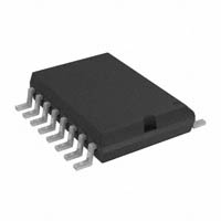
文档中提供了16-Pin SOIC(宽体)和14-Pin Plastic DIP/CerDIP的引脚配置图。

### 参数特性 - 高峰值输出电流:1.2A - 宽工作电压范围:4.5至18V - 对称的上升和下降时间:25ns - 短且相等的延迟时间:75ns - 防止感应电流反冲:500mA - 抗静电放电保护:2kV ESD保护所有引脚

### 功能详解 TC446X系列不会在任何条件下锁定,并且能够在地面线上出现高达5V的噪声尖峰时不受损。它们可以接受高达500mA的感性回弹电流而不损坏或逻辑扰动。此外,所有终端都至少有2000V的ESD保护。

### 应用信息 - 通用CMOS逻辑缓冲器,用于驱动所有四个MOSFET在H桥中的应用 - 直接小型电机驱动器、继电器或外设驱动器 - CCD驱动器 - 引脚开关网络驱动器

### 封装信息 - TC446xCOE:16-Pin SOIC(宽体),工作温度范围0°C至+70°C - TC446xCPD:14-Pin Plastic DIP,工作温度范围0至+70°C - TC446xEJD:14-Pin CerDIP,工作温度范围-40°C至+85°C - TC446xMJD:14-Pin CerDIP,工作温度范围-55°C至+125°C
TC4469COE 价格&库存

很抱歉,暂时无法提供与“TC4469COE”相匹配的价格&库存,您可以联系我们找货

免费人工找货