Bulletin PD-20783 07/04
10BQ030PbF
1 Amp
SCHOTTKY RECTIFIER
IF(AV) = 1.0Amp
VR = 30V
Major Ratings and Characteristics
Description/ Features
The 10BQ030PbF surface-mount Schottky rectifier has been
designed for applications requiring low forward drop and
small foot prints on PC boards. Typical applications are in disk
drives, switching power supplies, converters, free-wheeling
diodes, battery charging, and reverse battery protection.
Characteristics
Value
Units
IF(AV) Rectangular
waveform
1.0
A
VRRM
30
V
Small foot print, surface mountable
Very low forward voltage drop
IFSM @ tp= 5 ms sine
430
A
High frequency operation
VF
@ 1.0Apk, TJ= 125°C
0.30
V
Guard ring for enhanced ruggedness and long term
reliability
Lead-Free ("PbF" suffix)
TJ
range
- 55 to 150
°C
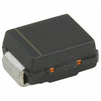
Case Styles
10BQ030PbF
SMB
Document Number: 94111
www.vishay.com
1
�10BQ030PbF
Bulletin PD-20783 07/04
Voltage Ratings
Part number
VR
10BQ030PbF
Max. DC Reverse Voltage (V)
30
VRWM Max. Working Peak Reverse Voltage (V)
Absolute Maximum Ratings
Parameters
10BQ
Units
IF(AV) Max. Average Forward Current
1.0
A
IFSM
430
Max. Peak One Cycle Non-Repetitive
Surge Current * See Fig. 6
90
EAS
Non-Repetitive Avalanche Energy
3.0
mJ
IAR
Repetitive Avalanche Current
1.0
A
Conditions
50% duty cycle @ T L = 106 °C, rectangular wave form.
Following any rated
5µs Sine or 3µs Rect. pulse
load condition and
10ms Sine or 6ms Rect. pulse with rated V RRM applied
TJ = 25 °C, IAS = 1A, L = 6mH
Current decaying linearly to zero in 1 µsec
Frequency limited by T J max. Va = 1.5 x Vr typical
Electrical Specifications
Parameters
VFM
VFM
Max. Forward Voltage Drop
Max. Forward Voltage Drop
(1)
(1)
10BQ
Units
0.420
V
@ 1A
Conditions
0.470
V
@ 2A
0.300
V
@ 1A
0.370
V
@ 2A
0.5
mA
TJ = 25 °C
TJ = 100 °C
TJ = 25 °C
TJ = 125 °C
VR = rated V R
IRM
Max. Reverse Leakage Current (1)
5.0
mA
15
mA
TJ = 125 °C
CT
Max. Junction Capacitance
200
pF
VR = 5VDC (test signal range 100KHz to 1Mhz) 25°C
LS
Typical Series Inductance
2.0
nH
Measured lead to lead 5mm from package body
10000
V/µs
dv/dt Max. Voltage Rate of Change
(Rated VR)
(1) Pulse Width < 300µs, Duty Cycle < 2%
Thermal-Mechanical Specifications
Parameters
10BQ
Units
TJ
Max. Junction Temperature Range (*) - 55 to 150
°C
Tstg
Max. Storage Temperature Range
°C
- 55 to 150
Conditions
RthJL Max. Thermal Resistance Junction
to Lead
(**)
25
°C/W DC operation
RthJA Max. Thermal Resistance Junction
to Ambient
wt
Approximate Weight
80
°C/W
0.10 (0.003) g (oz.)
Case Style
SMB
Device Marking
IR1E
(*) dPtot
dTj
<
1
Rth( j-a)
Similar DO-214AA
thermal runaway condition for a diode on its own heatsink
(**) Mounted 1 inch square PCB
Document Number: 94111
www.vishay.com
2
�10BQ030PbF
Bulletin PD-20783 07/04
10
TJ = 125°C
1
100°C
75°C
0.1
50°C
0.01
25°C
0.001
0.0001
0
10
20
TJ = 125°C
Reverse Voltage - VR (V)
TJ = 25°C
Fig. 2 - Typical Peak Reverse Current
Vs. Reverse Voltage
1
30
1000
0.1
0
0.2
0.4
0.6
0.8
Forward Voltage Drop - V FM (V)
Fig. 1 - Maximum Forward Voltage Drop Characteristics
Junction Capa citance - C T (pF)
Insta ntaneous Forward Current - IF (A)
Reverse Current - IR (mA)
10
TJ = 25°C
100
10
0
10
20
30
Reverse Voltage - VR (V)
Fig. 3 - Typical Junction Capacitance
Vs. Reverse Voltage
Document Number: 94111
www.vishay.com
3
�10BQ030PbF
Bulletin PD-20783 07/04
0.5
DC
Average Power Loss - (Watts)
Allowable Case Temperature - (°C)
130
120
D = 0.20
D = 0.25
D = 0.33
D = 0.50
D = 0.75
110
100
Square wave (D = 0.50)
80% Rated VR applied
D = 0.20
D = 0.25
D = 0.33
D = 0.50
D = 0.75
0.4
0.3
DC
RMSLimit
0.2
0.1
see note (2)
90
0
0
0.4
0.8
1.2
0
1.6
Average Forward Current - I F(AV) (A)
0.8
1.2
1.6
Fig. 5 - Maximum Average Forward Dissipation
Vs. Average Forward Current
Fig. 4 - Maximum Average Forward Current
Vs. Allowable Lead Temperature
Non-Repetitive Surge Current - I FSM (A)
0.4
Average Forward Current - I F(AV) (A)
1000
100
At Any Ra ted Load Condition
And With Rated VRRM Applied
Following Surge
10
10
100
1000
10000
Square Wave Pulse Duration - t p (microsec)
Fig. 6 - Maximum Peak Surge Forward Current Vs. Pulse Duration
(2) Formula used: TC = TJ - (Pd + PdREV) x RthJC ;
Pd = Forward Power Loss = IF(AV) x VFM @ (IF(AV) / D) (see Fig. 6);
PdREV = Inverse Power Loss = V R1 x IR (1 - D); IR @ VR1 = 80% rated VR
Document Number: 94111
www.vishay.com
4
�10BQ030PbF
Bulletin PD-20783 07/04
Outline Table
CATHODE
Device Marking: IR1E
2.15 (.085)
1.80 (.071)
1
3.80 (.150)
3.30 (.130)
1
4.70 (.185)
POLARITY
ANODE
2
2 PART NUMBER
4.10 (.161)
2.5 TYP.
(.098 TYP.)
2.40 (.094)
1.90 (.075)
0.30 (.012)
0.15 (.006)
1.30 (.051)
0.76 (.030)
5.60 (.220)
5.00 (.197)
2.0 TYP.
(.079 TYP.)
SOLDERING PAD
4.2 (.165)
4.0 (.157)
Outline SMB
Dimensions in millimeters and (inches)
For recommended footprint and soldering techniques refer to application note #AN-994
Marking & Identification
Each device has 2 rows for identification. The first row designates the device as manufactured by International
Rectifier, indicated by the letters "IR", and the Part Number (indicates the current, the voltage rating and
Schottky Generation). The second row indicates the year, the week of manufacturing and the Site ID.
IR1E
VOLTAGE
CURRENT
IR LOGO
PYWWX
SITE ID
WEEK
2nd digit of the YEAR
"Y" = 1st digit of the YEAR "standard product"
"P" = "Lead-Free"
Document Number: 94111
www.vishay.com
5
�10BQ030PbF
Bulletin PD-20783 07/04
Tape & Reel Information
Dimensions in millimetres and (inches)
Ordering Information Table
Device Code
10
B
Q
030
1
2
3
4
TR PbF
5
6
1
-
Current Rating
2
-
B = Single Lead Diode
3
-
Q = Schottky Q Series
4
-
Voltage Rating (030 = 30V)
5
-
y none = Box (1000 pieces)
6
-
y TR = Tape & Reel (3000 pieces)
y none = Standard Production
y PbF = Lead-Free
Data and specifications subject to change without notice.
This product has been designed and qualified for Industrial Level and Lead-Free.
Qualification Standards can be found on IR's Web site.
IR WORLD HEADQUARTERS: 233 Kansas St., El Segundo, California 90245, USA Tel: (310) 252-7105
TAC Fax: (310) 252-7309
07/04
Document Number: 94111
www.vishay.com
6
�Legal Disclaimer Notice
Vishay
Notice
The products described herein were acquired by Vishay Intertechnology, Inc., as part of its acquisition of
International Rectifier’s Power Control Systems (PCS) business, which closed in April 2007. Specifications of the
products displayed herein are pending review by Vishay and are subject to the terms and conditions shown below.
Specifications of the products displayed herein are subject to change without notice. Vishay Intertechnology, Inc., or
anyone on its behalf, assumes no responsibility or liability for any errors or inaccuracies.
Information contained herein is intended to provide a product description only. No license, express or implied, by
estoppel or otherwise, to any intellectual property rights is granted by this document. Except as provided in Vishay's
terms and conditions of sale for such products, Vishay assumes no liability whatsoever, and disclaims any express
or implied warranty, relating to sale and/or use of Vishay products including liability or warranties relating to fitness
for a particular purpose, merchantability, or infringement of any patent, copyright, or other intellectual property right.
The products shown herein are not designed for use in medical, life-saving, or life-sustaining applications.
Customers using or selling these products for use in such applications do so at their own risk and agree to fully
indemnify Vishay for any damages resulting from such improper use or sale.
Document Number: 99901
Revision: 08-Mar-07
www.vishay.com
1
�
很抱歉,暂时无法提供与“10BQ030TR”相匹配的价格&库存,您可以联系我们找货
免费人工找货