Bulletin PD-20530 rev. H 05/06
10WQ045FN
SCHOTTKY RECTIFIER
10 Amp
IF(AV) = 10Amp
VR = 45V
Major Ratings and Characteristics
Description/ Features
The 10WQ045FN surface mount Schottky rectifier has been
designed for applications requiring low forward drop and small
foot prints on PC board. Typical applications are in disk drives,
switching power supplies, converters, free-wheeling diodes,
battery charging, and reverse battery protection.
Characteristics
Values
Units
IF(AV) Rectangular
10
A
VRRM
45
V
Popular D-PAK outline
IFSM @ tp = 5 μs sine
400
A
Small foot print, surface moutable
Low forward voltage drop
VF
@10 Apk, TJ = 125°C
0.53
V
TJ
range
- 40 to 175
°C
waveform
High frequency operation
Guard ring for enhanced ruggedness and long term
reliability
Case Styles
Base
Cathode
4, 2
1
Anode
3
Anode
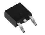
D-PAK (TO-252AA)
Document Number: 93199
www.vishay.com
1
�10WQ045FN
Bulletin PD-20530 rev. H 05/06
Voltage Ratings
Part number
VR
10WQ045FN
Max. DC Reverse Voltage (V)
45
VRWM Max. Working Peak Reverse Voltage (V)
Absolute Maximum Ratings
Parameters
10WQ...
IF(AV) Max. Average Forward Current
10
Units
A
Conditions
50% duty cycle @ TC = 157°C, rectangular wave form
* See Fig. 5
IFSM
Max. Peak One Cycle Non-Repet.
400
Surge Current * See Fig. 7
75
A
EAS
Non-RepetitiveAvalancheEnergy
20
mJ
IAR
Repetitive Avalanche Current
3.0
A
10WQ...
Units
5μs Sine or 3μs Rect. pulse
10ms Sine or 6ms Rect. pulse
Following any rated
load condition and with
rated VRRM applied
TJ = 25 °C, IAS = 3.0 Amps, L = 4.40 mH
Current decaying linearly to zero in 1 μsec
Frequency limited by TJ max. VA = 1.5 x VR typical
Electrical Specifications
Parameters
VFM
IRM
Conditions
Max. Forward Voltage Drop
0.630
V
@ 10A
* See Fig. 1
0.800
V
@ 20A
(1)
Max. Reverse Leakage Current
* See Fig. 2
(1)
VF(TO) Threshold Voltage
0.530
V
@ 10A
0.710
V
@ 20A
1
mA
TJ = 25 °C
15
mA
TJ = 125 °C
0.255
V
TJ = TJ max.
TJ = 25 °C
TJ = 125 °C
VR = rated VR
rt
Forward Slope Resistance
22
mΩ
CT
Typical Junction Capacitance
760
pF
V R = 5V DC (test signal range 100Khz to 1Mhz) 25 °C
LS
Typical Series Inductance
5.0
nH
Measured lead to lead 5mm from package body
(1) Pulse Width < 300μs, Duty Cycle < 2%
Thermal-Mechanical Specifications
Parameters
10WQ...
Units
TJ
Max. Junction Temp. Range (*)
- 40 to 175
°C
Tstg
Max. Storage Temperature Range
- 40 to 175
°C
2.0
°C/W
50
°C/W
0.3 (0.01)
g (oz.)
RthJC Max. Thermal Resistance Junction
to Case
RthJA Max. Thermal Resistance Junction
Conditions
DC operation
* See Fig. 4
to Ambient
wt
Approximate Weight
Case Style
D - PAK
Marking Device
(*) dPtot
dTj
<
1
Rth( j-a)
Similar to TO-252AA
10WQ045FN
thermal runaway condition for a diode on its own heatsink
Document Number: 93199
www.vishay.com
2
�10WQ045FN
Bulletin PD-20530 rev. H 05/06
1000
100
T = 175˚C
J
Reverse Current (mA)
150˚C
125˚C
10
100˚C
1
75˚C
0.1
50˚C
0.01
25˚C
0.001
0.0001
10
T J = 175˚C
0.2 0.4 0.6 0.8 1 1.2 1.4 1.6 1.8
Forward Voltage Drop - VFM (V)
20
30
40
50
10000
T J = 25˚C
0
10
Fig. 2 - Typical Values of Reverse Current
Vs. Reverse Voltage
T J = 125˚C
1
0
Reverse Voltage - VR (V)
Junction Capacitance - C T (pF)
Instantaneous Forward Current - I F (A)
100
T J = 25˚C
1000
100
2
0
10
20
30
40
50
Reverse Voltage - V R (V)
Fig. 1 - Maximum Forward Voltage Drop Characteristics
Fig. 3 - Typical Junction Capacitance
Vs. Reverse Voltage
Thermal Impedance - Z thJC (°C/W)
10
1
D = 0.75
D = 0.50
D = 0.33
D = 0.25
D = 0.20
0.1
Notes:
Single Pulse
(Thermal Resistance)
0.01
0.00001
1. Duty factor D = t1/ t2
2. Peak Tj = Pdm x ZthJC + Tc
0.0001
0.001
0.01
0.1
1
10
t1, Rectangular Pulse Duration (Seconds)
Fig. 4 - Maximum Thermal Impedance ZthJC Characteristics
Document Number: 93199
www.vishay.com
3
�10WQ045FN
Bulletin PD-20530 rev. H 05/06
10
170
Average Power Loss (Watts)
Allowable Case Temperature (°C)
180
DC
160
Square wave (D = 0.50)
80% Rated Vr applied
150
see note (2)
140
0
2
4
6
8
6
RMS Limit
4
DC
2
0
3
6
9
12
15
Average Forward Current - I F(AV) (A)
Average Forward Current - I F(AV) (A)
Fig. 6 - Forward Power Loss Characteristics
Fig. 5 - Maximum Allowable Case Temperature
Vs. Average Forward Current
1000
Non-Repetitive Surge Current - I
FSM
(A)
8
0
10 12 14 16
D = 0.20
D = 0.25
D = 0.33
D = 0.50
D = 0.75
100
At Any Rated Load Condition
And With Rated Vrrm Applied
Following Surge
10
10
100
1000
10000
Square Wave Pulse Duration - t p (microsec)
Fig. 7 - Maximum Non-Repetitive Surge Current
(2) Formula used: TC = TJ - (Pd + PdREV) x RthJC ;
Pd = Forward Power Loss = IF(AV) x VFM @ (IF(AV) / D) (see Fig. 6);
PdREV = Inverse Power Loss = VR1 x IR (1 - D); IR @ VR1 = 80% rated VR
Document Number: 93199
www.vishay.com
4
�10WQ045FN
Bulletin PD-20530 rev. H 05/06
Outline Table
Modified JEDEC outline TO-252AA
Dimensions in millimeters and (inches)
Part Marking Information
THIS IS A 10WQ045FN
INTERNATIONAL
RECTIFIER
LOT CODE 8024
LOGO
ASSEMBLED ON WW 02, 2000
ASSEMBLY
LOT CODE
Document Number: 93199
PART NUMBER
10WQ045FN
DATE CODE
YEAR 0 = 2000
WEEK 02
X = SITE ID
www.vishay.com
5
�10WQ045FN
Bulletin PD-20530 rev. H 05/06
Tape & Reel Information
TR
4.1 (0.16)
3.9 (0.15)
1.85 (0.07)
DIA.
1.65 (0.06)
2.1 (0.83)
1.9 (0.07)
1.85 (0.07)
1.65 (0.06)
0.35 (0.01)
0.25 (0.01)
7.6 (0.30)
7.4 (0.29)
FEED DIRECTION
12.1 (0.48)
11.9 (0.47)
4.1 (0.16)
3.9 (0.15)
TRR
2.1 (0.83)
1.9 (0.07)
2.6 (0.10)
DIA.
1.5 (0.06)
1.85 (0.07)
DIA.
1.65 (0.06)
1.85 (0.07)
1.65 (0.06)
7.6 (0.30)
7.4 (0.29)
FEED DIRECTION
8.1 (0.32)
7.9 (0.31)
4.1 (0.16)
3.9 (0.15)
TRL
2.1 (0.83)
1.9 (0.07)
2.6 (0.10)
DIA.
1.5 (0.06)
1.85 (0.07)
DIA.
1.65 (0.06)
1.85 (0.07)
1.65 (0.06)
7.6 (0.30)
7.4 (0.29)
FEED DIRECTION
13 (0.52) DIA.
8.1 (0.32)
7.9 (0.31)
2.6 (0.10)
DIA.
1.5 (0.06)
7.0 (0.28)
6.8 (0.26)
16.3 (0.64)
15.7 (0.62)
2.75 (0.11)
2.55 (0.10)
0.35 (0.01)
0.25 (0.01)
10.6 (0.42)
10.4 (0.41)
16.3 (0.64)
15.7 (0.62)
2.75 (0.11)
2.55 (0.10)
0.35 (0.01)
0.25 (0.01)
10.6 (0.42)
10.4 (0.41)
16.3 (0.64)
15.7 (0.62)
2.75 (0.11)
2.55 (0.10)
22.4 (0.88)
TO-252AA Tape & Reel
375 (14.17)
DIA. MAX.
Document Number: 93199
50 (1.97) DIA.
When ordering, indicate the part
number, part orientation, and the
quantity. Quantities are in multiples
of 2,000 pieces per reel for TR and
multiples of 3,000 pieces per reel
for both TRL and TRR.
www.vishay.com
6
�10WQ045FN
Bulletin PD-20530 rev. H 05/06
Ordering Information Table
Device Code
10
W
Q
1
2
3
1
-
2
-
045 FN TRL
4
5
6
7
Current Rating (10A)
Package Identifier
W = D-Pak
4
3
-
Schottky "Q" Series
4
-
Voltage Rating (045 = 45V)
5
-
FN = TO-252AA
6
-
y none = Tube (50 pieces)
y TR = Tape & Reel
y TRL = Tape & Reel (Left Oriented)
y TRR = Tape & Reel (Right Oriented)
7
-
y none = Standard Production
y PbF = Lead-Free
Data and specifications subject to change without notice.
This product has been designed and qualified for AEC Q101 Level.
Qualification Standards can be found on IR's Web site.
IR WORLD HEADQUARTERS: 233 Kansas St., El Segundo, California 90245, USA Tel: (310) 252-7105
TAC Fax: (310) 252-7309
05/06
Document Number: 93199
www.vishay.com
7
�Legal Disclaimer Notice
Vishay
Notice
The products described herein were acquired by Vishay Intertechnology, Inc., as part of its acquisition of
International Rectifier’s Power Control Systems (PCS) business, which closed in April 2007. Specifications of the
products displayed herein are pending review by Vishay and are subject to the terms and conditions shown below.
Specifications of the products displayed herein are subject to change without notice. Vishay Intertechnology, Inc., or
anyone on its behalf, assumes no responsibility or liability for any errors or inaccuracies.
Information contained herein is intended to provide a product description only. No license, express or implied, by
estoppel or otherwise, to any intellectual property rights is granted by this document. Except as provided in Vishay's
terms and conditions of sale for such products, Vishay assumes no liability whatsoever, and disclaims any express
or implied warranty, relating to sale and/or use of Vishay products including liability or warranties relating to fitness
for a particular purpose, merchantability, or infringement of any patent, copyright, or other intellectual property right.
The products shown herein are not designed for use in medical, life-saving, or life-sustaining applications.
Customers using or selling these products for use in such applications do so at their own risk and agree to fully
indemnify Vishay for any damages resulting from such improper use or sale.
International Rectifier®, IR®, the IR logo, HEXFET®, HEXSense®, HEXDIP®, DOL®, INTERO®, and POWIRTRAIN®
are registered trademarks of International Rectifier Corporation in the U.S. and other countries. All other product
names noted herein may be trademarks of their respective owners.
Document Number: 99901
Revision: 12-Mar-07
www.vishay.com
1
�