BPW41N
www.vishay.com
Vishay Semiconductors
Silicon PIN Photodiode
FEATURES
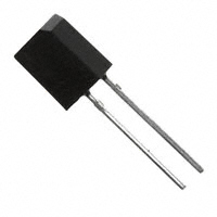
• Package type: leaded
• Package form: side view
• Dimensions (in mm): 5 x 4 x 6.8
• Radiant sensitive area (in mm2): 7.5
• High radiant sensitivity
• Daylight blocking filter matched with 940 nm
emitters
• Fast response times
94 8480
• Angle of half sensitivity: ϕ = ± 65°
• Compliant to RoHS Directive to 2002/95/EC and in
accordance to WEEE 2002/96/EC
Note
** Please see document “Vishay Material Category Policy”:
www.vishay.com/doc?99902
DESCRIPTION
BPW41N is a PIN photodiode with high speed and high
radiant sensitivity in a black, side view plastic package with
daylight blocking filter. Filter bandwidth is matched with
900 nm to 950 nm IR emitters.
APPLICATIONS
• High speed detector for infrared radiation
• Infrared remote control and free air data transmission
systems, e.g. in combination with TSALxxxx series IR
emitters
PRODUCT SUMMARY
COMPONENT
Ira (μA)
ϕ (deg)
λ0.5 (nm)
45
± 65
870 to 1050
PACKAGING
REMARKS
PACKAGE FORM
Bulk
MOQ: 4000 pcs, 4000 pcs/bulk
Side view
BPW41N
Note
• Test condition see table “Basic Characteristics”
ORDERING INFORMATION
ORDERING CODE
BPW41N
Note
• MOQ: minimum order quantity
ABSOLUTE MAXIMUM RATINGS (Tamb = 25 °C, unless otherwise specified)
PARAMETER
TEST CONDITION
Reverse voltage
Power dissipation
Tamb ≤ 25 °C
Junction temperature
Operating temperature range
Thermal resistance junction/ambient
Rev. 1.6, 23-Aug-11
VALUE
VR
60
UNIT
V
PV
215
mW
Tj
100
°C
Tamb
- 40 to + 100
°C
°C
Tstg
- 40 to + 100
t≤5s
Tsd
260
°C
Connected with Cu wire, 0.14 mm2
RthJA
350
K/W
Storage temperature range
Soldering temperature
SYMBOL
Document Number: 81522
1
For technical questions, contact: detectortechsupport@vishay.com
THIS DOCUMENT IS SUBJECT TO CHANGE WITHOUT NOTICE. THE PRODUCTS DESCRIBED HEREIN AND THIS DOCUMENT
ARE SUBJECT TO SPECIFIC DISCLAIMERS, SET FORTH AT www.vishay.com/doc?91000
�BPW41N
www.vishay.com
Vishay Semiconductors
BASIC CHARACTERISTICS (Tamb = 25 °C, unless otherwise specified)
PARAMETER
TEST CONDITION
SYMBOL
MIN.
Breakdown voltage
IR = 100 μA, E = 0
V(BR)
60
MAX.
UNIT
V
VR = 10 V, E = 0
Iro
2
VR= 0 V, f = 1 MHz, E = 0
CD
70
VR= 3 V, f = 1 MHz, E = 0
CD
25
Reverse dark current
Diode capacitance
TYP.
30
nA
40
pF
pF
Open circuit Voltage
Ee = 1 mW/cm2, λ = 950 nm
Vo
350
mV
Temperature coefficient of Vo
Ee = 1 mW/cm2, λ = 950 nm
TKVo
- 2.6
mV/K
Short circuit current
Ee = 1 mW/cm2, λ = 950 nm
Ik
38
μA
Temperature coefficient of Ik
Ee = 1 mW/cm2, λ = 950 nm
TKIk
0.1
%/K
Reverse light current
Ee = 1 mW/cm2, λ = 950 nm,
VR = 5 V
45
μA
43
Ira
Angle of half sensitivity
ϕ
± 65
deg
Wavelength of peak sensitivity
λp
950
nm
λ0.5
870 to 1050
nm
VR = 10 V, λ = 950 nm
NEP
4 x 10-14
W/√ Hz
Rise time
VR = 10 V, RL = 1 kΩ, λ = 820 nm
tr
100
ns
Fall time
VR = 10 V, RL = 1 kΩ, λ = 820 nm
tf
100
ns
Range of spectral bandwidth
Noise equivalent power
100
1.4
VR = 5 V
λ = 950 nm
1.2
1 mW/cm2
I ra - Reverse Light Current (µA)
I ra rel - Relative Reverse Light Current
BASIC CHARACTERISTICS (Tamb = 25 °C, unless otherwise specified)
1.0
0.8
0.5 mW/cm2
λ = 950 nm
0.1 mW/cm2
0.05 mW/cm2
0.02 mW/cm2
1
0.6
0
94 8409
20
40
60
80
0.1
100
Tamb - Ambient Temperature (°C)
94 8415
Fig. 1 - Relative Reverse Light Current vs. Ambient Temperature
CD - Diode Capacitance (pF)
10
VR = 5 V
λ = 950 nm
1
94 8414
0.1
1
10
E e - Irradiance (mW/cm²)
Fig. 2 - Reverse Light Current vs. Irradiance
Rev. 1.6, 23-Aug-11
10
100
80
100
0.1
0.01
1
V R - Reverse Voltage (V)
Fig. 3 - Reverse Light Current vs. Reverse Voltage
1000
Ira - Reverse Light Current (µA)
0.2 mW/cm2
10
E=0
f = 1 MHz
60
40
20
0
0.1
948407
1
10
100
VR - Reverse Voltage (V)
Fig. 4 - Diode Capacitance vs. Reverse Voltage
Document Number: 81522
2
For technical questions, contact: detectortechsupport@vishay.com
THIS DOCUMENT IS SUBJECT TO CHANGE WITHOUT NOTICE. THE PRODUCTS DESCRIBED HEREIN AND THIS DOCUMENT
ARE SUBJECT TO SPECIFIC DISCLAIMERS, SET FORTH AT www.vishay.com/doc?91000
�BPW41N
www.vishay.com
Vishay Semiconductors
10°
20°
1.0
0.8
0.6
0.4
0.2
0
750
850
950
0.9
50°
0.8
60°
70°
0.7
80°
0.6
1150
1050
λ - Wavelength (nm)
94 8408
40°
1.0
ϕ - Angular Displacement
30°
Srel - Relative Radiant Sensitivity
S (λ)rel - Relative Spectral Sensitivity
0°
1.2
0.4
0.2
0
94 8406
Fig. 5 - Relative Spectral Sensitivity vs. Wavelength
Fig. 6 - Relative Radiant Sensitivity vs. Angular Displacement
PACKAGE DIMENSIONS in millimeters
± 0.2
4
± 0.2
5
C
6.8
< 0.5
± 0.3
Chip position
(2.05)
19.8
- 0.8
8.9
± 0.3
Sensitive area
(2.8)
A
Area not plane
< 0.65
0.45
+ 0.01
- 0.05
2.5 nom.
Drawing-No.: 6.544-5108.01-4
2.3
0.4
± 0.2
+ 0.1
- 0.05
technical drawings
according to DIN
specifications
Issue:1; 01.07.96
96 12195
Rev. 1.6, 23-Aug-11
Document Number: 81522
3
For technical questions, contact: detectortechsupport@vishay.com
THIS DOCUMENT IS SUBJECT TO CHANGE WITHOUT NOTICE. THE PRODUCTS DESCRIBED HEREIN AND THIS DOCUMENT
ARE SUBJECT TO SPECIFIC DISCLAIMERS, SET FORTH AT www.vishay.com/doc?91000
�Legal Disclaimer Notice
www.vishay.com
Vishay
Disclaimer
ALL PRODUCT, PRODUCT SPECIFICATIONS AND DATA ARE SUBJECT TO CHANGE WITHOUT NOTICE TO IMPROVE
RELIABILITY, FUNCTION OR DESIGN OR OTHERWISE.
Vishay Intertechnology, Inc., its affiliates, agents, and employees, and all persons acting on its or their behalf (collectively,
“Vishay”), disclaim any and all liability for any errors, inaccuracies or incompleteness contained in any datasheet or in any other
disclosure relating to any product.
Vishay makes no warranty, representation or guarantee regarding the suitability of the products for any particular purpose or
the continuing production of any product. To the maximum extent permitted by applicable law, Vishay disclaims (i) any and all
liability arising out of the application or use of any product, (ii) any and all liability, including without limitation special,
consequential or incidental damages, and (iii) any and all implied warranties, including warranties of fitness for particular
purpose, non-infringement and merchantability.
Statements regarding the suitability of products for certain types of applications are based on Vishay’s knowledge of
typical requirements that are often placed on Vishay products in generic applications. Such statements are not binding
statements about the suitability of products for a particular application. It is the customer’s responsibility to validate that a
particular product with the properties described in the product specification is suitable for use in a particular application.
Parameters provided in datasheets and / or specifications may vary in different applications and performance may vary over
time. All operating parameters, including typical parameters, must be validated for each customer application by the customer’s
technical experts. Product specifications do not expand or otherwise modify Vishay’s terms and conditions of purchase,
including but not limited to the warranty expressed therein.
Except as expressly indicated in writing, Vishay products are not designed for use in medical, life-saving, or life-sustaining
applications or for any other application in which the failure of the Vishay product could result in personal injury or death.
Customers using or selling Vishay products not expressly indicated for use in such applications do so at their own risk.
Please contact authorized Vishay personnel to obtain written terms and conditions regarding products designed for
such applications.
No license, express or implied, by estoppel or otherwise, to any intellectual property rights is granted by this document
or by any conduct of Vishay. Product names and markings noted herein may be trademarks of their respective owners.
© 2017 VISHAY INTERTECHNOLOGY, INC. ALL RIGHTS RESERVED
Revision: 08-Feb-17
1
Document Number: 91000
�