BPW96B, BPW96C
www.vishay.com
Vishay Semiconductors
Silicon NPN Phototransistor
FEATURES
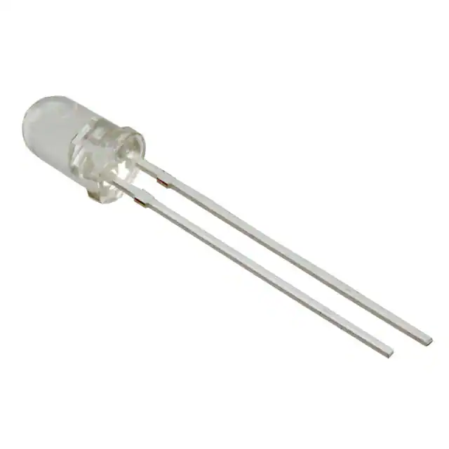
• Package type: leaded
• Package form: T-1¾
• Dimensions (in mm): Ø 5
• Leads with stand-off
• High photo sensitivity
• High radiant sensitivity
• Suitable for visible and near infrared radiation
94 8391
• Fast response times
• Angle of half sensitivity: ϕ = ± 20°
• Compliant to RoHS Directive 2002/95/EC and in
accordance to WEEE 2002/96/EC
DESCRIPTION
BPW96 is a silicon NPN phototransistor with high radiant
sensitivity in clear, T-1¾ plastic package. It is sensitive to
visible and near infrared radiation.
Note
** Please see document “Vishay Material Category Policy”:
www.vishay.com/doc?99902
APPLICATIONS
• Detector in electronic control and drive circuits
PRODUCT SUMMARY
Ica (mA)
ϕ (deg)
λ0.1 (nm)
BPW96B
2.5 to 7.5
± 20
450 to 1080
BPW96C
4.5 to 15
± 20
450 to 1080
PACKAGING
REMARKS
PACKAGE FORM
BPW96B
Bulk
MOQ: 4000 pcs, 4000 pcs/bulk
T-1¾
BPW96C
Bulk
MOQ: 4000 pcs, 4000 pcs/bulk
T-1¾
COMPONENT
Note
• Test condition see table “Basic Characteristics”
ORDERING INFORMATION
ORDERING CODE
Note
• MOQ: minimum order quantity
ABSOLUTE MAXIMUM RATINGS (Tamb = 25 °C, unless otherwise specified)
SYMBOL
VALUE
Collector emitter voltage
PARAMETER
TEST CONDITION
VCEO
70
V
Emitter collector voltage
VECO
5
V
Collector current
UNIT
IC
50
mA
tp/T ≤ 0.5, tp ≤ 10 ms
ICM
100
mA
Tamb ≤ 47 °C
PV
150
mW
Tj
100
°C
Operating temperature range
Tamb
- 40 to + 100
°C
Storage temperature range
Tstg
- 40 to + 100
°C
t≤3s
Tsd
260
°C
Connected with Cu wire, 0.14 mm2
RthJA
350
K/W
Collector peak current
Power dissipation
Junction temperature
Soldering temperature
Thermal resistance junction/ambient
Rev. 1.8, 23-Aug-11
Document Number: 81532
1
For technical questions, contact: detectortechsupport@vishay.com
THIS DOCUMENT IS SUBJECT TO CHANGE WITHOUT NOTICE. THE PRODUCTS DESCRIBED HEREIN AND THIS DOCUMENT
ARE SUBJECT TO SPECIFIC DISCLAIMERS, SET FORTH AT www.vishay.com/doc?91000
�BPW96B, BPW96C
www.vishay.com
Vishay Semiconductors
PV - Power Dissipation (mW)
200
160
120
RthJA
80
40
0
0
94 8300
20
40
60
80
Tamb - Ambient Temperature (°C)
100
Fig. 1 - Power Dissipation Limit vs. Ambient Temperature
BASIC CHARACTERISTICS (Tamb = 25 °C, unless otherwise specified)
TEST CONDITION
SYMBOL
MIN.
IC = 1 mA
V(BR)CEO
70
Collector emitter dark current
VCE = 20 V, E = 0
ICEO
Collector emitter capacitance
VCE = 5 V, f = 1 MHz, E = 0
CCEO
3
pF
ϕ
± 20
deg
PARAMETER
Collector emitter breakdown voltage
Angle of half sensitivity
TYP.
MAX.
UNIT
1
200
nA
V
Wavelength of peak sensitivity
λp
850
nm
Range of spectral bandwidth
λ0.1
450 to 1080
nm
Ee = 1 mW/cm2, λ = 950 nm,
IC = 0.1 mA
VCEsat
Turn-on time
VS = 5 V, IC = 5 mA, RL = 100 Ω
ton
Turn-off time
VS = 5 V, IC = 5 mA, RL = 100 Ω
toff
2.3
μs
Cut-off frequency
VS = 5 V, IC = 5 mA, RL = 100 Ω
fc
180
kHz
Collector emitter saturation voltage
0.3
2.0
V
μs
TYPE DEDICATED CHARACTERISTICS
PARAMETER
Collector light current
Rev. 1.8, 23-Aug-11
TEST CONDITION
PART
SYMBOL
MIN.
TYP.
MAX.
UNIT
Ee = 1 mW/cm2, λ = 950 nm,
VCE = 5 V
BPW96B
Ica
2.5
4.5
7.5
mA
BPW96C
Ica
4.5
8
15
mA
Document Number: 81532
2
For technical questions, contact: detectortechsupport@vishay.com
THIS DOCUMENT IS SUBJECT TO CHANGE WITHOUT NOTICE. THE PRODUCTS DESCRIBED HEREIN AND THIS DOCUMENT
ARE SUBJECT TO SPECIFIC DISCLAIMERS, SET FORTH AT www.vishay.com/doc?91000
�BPW96B, BPW96C
www.vishay.com
Vishay Semiconductors
BASIC CHARACTERISTICS (Tamb = 25 °C, unless otherwise specified)
Ica - Collector Light Current (mA)
10
103
VCE = 20 V
102
101
10
20
40
60
Ica rel - Relative Collector Current
2.0
1.8
VCE = 5 V
Ee = 1 mW/cm2
λ = 950 nm
1.4
1.2
1.0
0.8
0.6
0
20
40
60
80
100
Tamb - Ambient Temperature (°C)
94 8239
1
100
10
V CE - Collector Emitter Voltage (V)
10
8
f = 1 MHz
6
4
2
0
0.1
1
100
10
V CE - Collector Emitter Voltage (V)
Fig. 5 - Collector Emitter Capacitance vs. Collector Emitter Voltage
ton/toff - Turn-on/Turn-off Time (µs)
Ica - Collector Light Current (mA)
λ = 950 nm
8
BPW96B
BPW96C
1
0.1
V CE = 5 V
λ = 950 nm
VCE = 5 V
RL = 100 Ω
λ = 950 nm
6
4
toff
2
ton
0
0.1
1
10
Ee - Irradiance (mW/cm2)
Fig. 3 - Collector Light Current vs. Irradiance
Rev. 1.8, 23-Aug-11
0.05 mW/cm²
Fig. 4 - Collector Light Current vs. Collector Emitter Voltage
10
94 8296
0.1 mW/cm²
94 8301
Fig. 2 - Relative Collector Current vs. Ambient Temperature
0.01
0.01
0.2 mW/cm²
1
94 8297
Fig. 1 - Collector Dark Current vs. Ambient Temperature
1.6
0.5 mW/cm²
0.1
0.1
100
80
Tamb - Ambient Temperature (°C)
94 8304
Ee = 1 mW/cm²
BPW96B
C CEO - Collector Emitter Capacitance (pF)
ICEO - Collector Dark Current (nA)
104
0
94 8293
2
4
6
8
10
12
14
IC - Collector Current (mA)
Fig. 6 - Turn-on/Turn-off Time vs. Collector Current
Document Number: 81532
3
For technical questions, contact: detectortechsupport@vishay.com
THIS DOCUMENT IS SUBJECT TO CHANGE WITHOUT NOTICE. THE PRODUCTS DESCRIBED HEREIN AND THIS DOCUMENT
ARE SUBJECT TO SPECIFIC DISCLAIMERS, SET FORTH AT www.vishay.com/doc?91000
�BPW96B, BPW96C
www.vishay.com
Vishay Semiconductors
10°
20°
0.8
0.6
0.4
0.2
40°
1.0
0.9
50°
0.8
60°
70°
0.7
ϕ - Angular Displacement
30°
1.0
Srel - Relative Radiant Sensitivity
S (λ)rel - Relative Spectral Sensitivity
0°
80°
0
400
600
800
1000
0.6
λ - Wavelength (nm)
94 8348
0.4
0.2
0
94 8299
Fig. 7 - Relative Spectral Sensitivity vs. Wavelength
Fig. 8 - Relative Radiant Sensitivity vs. Angular Displacement
5.75
± 0.15
PACKAGE DIMENSIONS in millimeters
C
E
Chip position
± 0.15
(4.8)
Ø5
± 0.15
7.6
± 0.3
2.4
0.8
Area not plane
+ 0.2
- 0.1
0.5
1.5
± 0.25
1
+ 0.2
- 0.1
< 0.7
35.3
± 0.5
8.6
± 0.3
R
12.3
re)
he
sp
5(
0.63
+ 0.15
+ 0.2
- 0.1
2.54 nom.
technical drawings
according to DIN
specifications
Drawing-No.: 6.544-5086.01-4
Issue:1; 01.07.96
96 12192
Rev. 1.8, 23-Aug-11
Document Number: 81532
4
For technical questions, contact: detectortechsupport@vishay.com
THIS DOCUMENT IS SUBJECT TO CHANGE WITHOUT NOTICE. THE PRODUCTS DESCRIBED HEREIN AND THIS DOCUMENT
ARE SUBJECT TO SPECIFIC DISCLAIMERS, SET FORTH AT www.vishay.com/doc?91000
�Legal Disclaimer Notice
www.vishay.com
Vishay
Disclaimer
ALL PRODUCT, PRODUCT SPECIFICATIONS AND DATA ARE SUBJECT TO CHANGE WITHOUT NOTICE TO IMPROVE
RELIABILITY, FUNCTION OR DESIGN OR OTHERWISE.
Vishay Intertechnology, Inc., its affiliates, agents, and employees, and all persons acting on its or their behalf (collectively,
“Vishay”), disclaim any and all liability for any errors, inaccuracies or incompleteness contained in any datasheet or in any other
disclosure relating to any product.
Vishay makes no warranty, representation or guarantee regarding the suitability of the products for any particular purpose or
the continuing production of any product. To the maximum extent permitted by applicable law, Vishay disclaims (i) any and all
liability arising out of the application or use of any product, (ii) any and all liability, including without limitation special,
consequential or incidental damages, and (iii) any and all implied warranties, including warranties of fitness for particular
purpose, non-infringement and merchantability.
Statements regarding the suitability of products for certain types of applications are based on Vishay's knowledge of typical
requirements that are often placed on Vishay products in generic applications. Such statements are not binding statements
about the suitability of products for a particular application. It is the customer's responsibility to validate that a particular product
with the properties described in the product specification is suitable for use in a particular application. Parameters provided in
datasheets and / or specifications may vary in different applications and performance may vary over time. All operating
parameters, including typical parameters, must be validated for each customer application by the customer's technical experts.
Product specifications do not expand or otherwise modify Vishay's terms and conditions of purchase, including but not limited
to the warranty expressed therein.
Hyperlinks included in this datasheet may direct users to third-party websites. These links are provided as a convenience and
for informational purposes only. Inclusion of these hyperlinks does not constitute an endorsement or an approval by Vishay of
any of the products, services or opinions of the corporation, organization or individual associated with the third-party website.
Vishay disclaims any and all liability and bears no responsibility for the accuracy, legality or content of the third-party website
or for that of subsequent links.
Except as expressly indicated in writing, Vishay products are not designed for use in medical, life-saving, or life-sustaining
applications or for any other application in which the failure of the Vishay product could result in personal injury or death.
Customers using or selling Vishay products not expressly indicated for use in such applications do so at their own risk. Please
contact authorized Vishay personnel to obtain written terms and conditions regarding products designed for such applications.
No license, express or implied, by estoppel or otherwise, to any intellectual property rights is granted by this document or by
any conduct of Vishay. Product names and markings noted herein may be trademarks of their respective owners.
© 2024 VISHAY INTERTECHNOLOGY, INC. ALL RIGHTS RESERVED
Document Number: 91000
1
For technical questions, contact:
THIS DOCUMENT IS SUBJECT TO CHANGE WITHOUT NOTICE. THE PRODUCTS DESCRIBED HEREIN AND THIS DOCUMENT
ARE SUBJECT TO SPECIFIC DISCLAIMERS, SET FORTH AT www.vishay.com/doc?91000
Revision: 01-Jan-2024
�