BYV98-50, BYV98-100, BYV98-150, BYV98-200
www.vishay.com
Vishay Semiconductors
Ultra-Fast Avalanche Sinterglass Diode
FEATURES
• High reverse voltage
• Glass passivated
• Low reverse current
• Low forward voltage drop
• Hermetically sealed axial-leaded glass envelope
• Material categorization:
for definitions of compliance please see
www.vishay.com/doc?99912
949588
DESIGN SUPPORT TOOLS
APPLICATIONS
click logo to get started
• Switched mode power supplies
Models
Available
MECHANICAL DATA
Case: SOD-64
Terminals: plated axial leads, solderable per MIL-STD-750,
method 2026
Polarity: color band denotes cathode end
• High-frequency inverter circuits
Mounting position: any
Weight: approx. 858 mg
ORDERING INFORMATION (Example)
DEVICE NAME
ORDERING CODE
TAPED UNITS
MINIMUM ORDER QUANTITY
BYV98-200
BYV98-200-TR
2500 per 10" tape and reel
12 500
BYV98-200
BYV98-200-TAP
2500 per ammopack
12 500
TYPE DIFFERENTIATION
PACKAGE
PARTS TABLE
PART
BYV98-50
VR = 50 V; IF(AV) = 4 A
SOD-64
BYV98-100
VR = 100 V; IF(AV) = 4 A
SOD-64
BYV98-150
VR = 150 V; IF(AV) = 4 A
SOD-64
BYV98-200
VR = 200 V; IF(AV) = 4 A
SOD-64
ABSOLUTE MAXIMUM RATINGS (Tamb = 25 °C, unless otherwise specified)
PARAMETER
Reverse voltage = repetitive peak reverse
voltage
Peak forward surge current
Average forward current
TEST CONDITION
PART
SYMBOL
VALUE
UNIT
BYV98-50
VR = VRRM
50
V
BYV98-100
VR = VRRM
100
V
BYV98-150
VR = VRRM
150
V
BYV98-200
VR = VRRM
200
V
tp = 10 ms, half sine wave
IFSM
70
A
Tamb = 30 °C, l = 10 mm
IF(AV)
4
A
Tj = Tstg
-55 to +175
°C
ER
20
mJ
See electrical characteristics
Junction and storage temperature range
Non repetitive reverse avalanche energy
l(BR)R = 1 A
Rev. 1.8, 21-Feb-18
Document Number: 86046
1
For technical questions within your region: DiodesAmericas@vishay.com, DiodesAsia@vishay.com, DiodesEurope@vishay.com
THIS DOCUMENT IS SUBJECT TO CHANGE WITHOUT NOTICE. THE PRODUCTS DESCRIBED HEREIN AND THIS DOCUMENT
ARE SUBJECT TO SPECIFIC DISCLAIMERS, SET FORTH AT www.vishay.com/doc?91000
�BYV98-50, BYV98-100, BYV98-150, BYV98-200
www.vishay.com
Vishay Semiconductors
MAXIMUM THERMAL RESISTANCE (Tamb = 25 °C, unless otherwise specified)
PARAMETER
Junction ambient
TEST CONDITION
SYMBOL
VALUE
UNIT
Lead length l = 10 mm, TL = constant
RthJA
25
K/W
ELECTRICAL CHARACTERISTICS (Tamb = 25 °C, unless otherwise specified)
PARAMETER
TEST CONDITION
Forward voltage
Reverse current
SYMBOL
MIN.
TYP.
MAX.
IF = 5 A
PART
VF
-
-
1.1
V
VR = VRRM
IR
-
-
10
μA
VR = VRRM, Tj = 150 °C
IR = 100 μA
Reverse breakdown voltage
IR
-
-
200
μA
BYV98-50
V(BR)R
60
-
-
V
BYV98-100
V(BR)R
120
-
-
V
BYV98-150
V(BR)R
170
-
-
V
BYV98-200
V(BR)R
220
-
-
V
trr
-
-
35
ns
IF = 0.5 A, IR = 1 A, iR = 0.25 A
Reverse recovery time
UNIT
TYPICAL CHARACTERISTICS (Tamb = 25 C, unless otherwise specified)
180
V R = VRRM
100
RthJA =
80
25 K/W
70 K/W
60
150 K/W
BYV98–200
BYV98–150
BYV98–100
40
BYV98–50
20
CD – Diode Capacitance ( pF )
PR – Reverse Power Dissipation ( mW)
120
160
140
120
100
80
60
40
20
0
25
15784
50
75
100 125 150 175
Tj – Junction Temperature ( °C )
0
0.1
Fig. 1 - Max. Reverse Power Dissipation vs. Junction Temperature
I R – Reverse Current (A)
100
10
1
50
75
100 125 150 175
Tj – Junction Temperature ( °C )
Fig. 2 - Max. Reverse Current vs. Junction Temperature
I FAV –Average Forward Current( A )
4.5
V R = VRRM
15785
100.0
Fig. 3 - Diode Capacitance vs. Reverse Voltage
1000
25
1.0
10.0
V R – Reverse Voltage ( V )
17194
V R = VRRM
half sinewave
4.0
3.5
R thJA = 25 K/W
l = 10 mm
3.0
2.5
2.0
1.5
1.0
R thJA = 70 K/W
PCB: d = 25 mm
0.5
0.0
0
15783
20
40 60 80 100 120 140 160 180
Tamb – Ambient Temperature ( °C )
Fig. 4 - Max. Average Forward Current vs. Ambient Temperature
Rev. 1.8, 21-Feb-18
Document Number: 86046
2
For technical questions within your region: DiodesAmericas@vishay.com, DiodesAsia@vishay.com, DiodesEurope@vishay.com
THIS DOCUMENT IS SUBJECT TO CHANGE WITHOUT NOTICE. THE PRODUCTS DESCRIBED HEREIN AND THIS DOCUMENT
ARE SUBJECT TO SPECIFIC DISCLAIMERS, SET FORTH AT www.vishay.com/doc?91000
�BYV98-50, BYV98-100, BYV98-150, BYV98-200
www.vishay.com
Vishay Semiconductors
100.00
IF – Forward Current (A)
T j = 175°C
10.00
Tj = 25 °C
1.00
0.10
0.01
0.0 0.5 1.0 1.5 2.0 2.5 3.0 3.5 4.0
V F – Forward Voltage ( V )
15782
Fig. 5 - Max. Forward Current vs. Forward Voltage
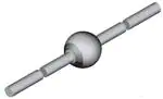
PACKAGE DIMENSIONS in millimeters (inches): SOD-64
Sintered Glass Case
SOD-64
Cathode Identification
4.3 (0.168) max.
1.35 (0.053) max.
26(1.014) min.
4 (0.156) max.
26 (1.014) min.
Document-No.: 6.563-5006.4-4
Rev. 3 - Date: 09.February.2005
94 9587
Rev. 1.8, 21-Feb-18
Document Number: 86046
3
For technical questions within your region: DiodesAmericas@vishay.com, DiodesAsia@vishay.com, DiodesEurope@vishay.com
THIS DOCUMENT IS SUBJECT TO CHANGE WITHOUT NOTICE. THE PRODUCTS DESCRIBED HEREIN AND THIS DOCUMENT
ARE SUBJECT TO SPECIFIC DISCLAIMERS, SET FORTH AT www.vishay.com/doc?91000
�Legal Disclaimer Notice
www.vishay.com
Vishay
Disclaimer
ALL PRODUCT, PRODUCT SPECIFICATIONS AND DATA ARE SUBJECT TO CHANGE WITHOUT NOTICE TO IMPROVE
RELIABILITY, FUNCTION OR DESIGN OR OTHERWISE.
Vishay Intertechnology, Inc., its affiliates, agents, and employees, and all persons acting on its or their behalf (collectively,
“Vishay”), disclaim any and all liability for any errors, inaccuracies or incompleteness contained in any datasheet or in any other
disclosure relating to any product.
Vishay makes no warranty, representation or guarantee regarding the suitability of the products for any particular purpose or
the continuing production of any product. To the maximum extent permitted by applicable law, Vishay disclaims (i) any and all
liability arising out of the application or use of any product, (ii) any and all liability, including without limitation special,
consequential or incidental damages, and (iii) any and all implied warranties, including warranties of fitness for particular
purpose, non-infringement and merchantability.
Statements regarding the suitability of products for certain types of applications are based on Vishay's knowledge of typical
requirements that are often placed on Vishay products in generic applications. Such statements are not binding statements
about the suitability of products for a particular application. It is the customer's responsibility to validate that a particular product
with the properties described in the product specification is suitable for use in a particular application. Parameters provided in
datasheets and / or specifications may vary in different applications and performance may vary over time. All operating
parameters, including typical parameters, must be validated for each customer application by the customer's technical experts.
Product specifications do not expand or otherwise modify Vishay's terms and conditions of purchase, including but not limited
to the warranty expressed therein.
Hyperlinks included in this datasheet may direct users to third-party websites. These links are provided as a convenience and
for informational purposes only. Inclusion of these hyperlinks does not constitute an endorsement or an approval by Vishay of
any of the products, services or opinions of the corporation, organization or individual associated with the third-party website.
Vishay disclaims any and all liability and bears no responsibility for the accuracy, legality or content of the third-party website
or for that of subsequent links.
Except as expressly indicated in writing, Vishay products are not designed for use in medical, life-saving, or life-sustaining
applications or for any other application in which the failure of the Vishay product could result in personal injury or death.
Customers using or selling Vishay products not expressly indicated for use in such applications do so at their own risk. Please
contact authorized Vishay personnel to obtain written terms and conditions regarding products designed for such applications.
No license, express or implied, by estoppel or otherwise, to any intellectual property rights is granted by this document or by
any conduct of Vishay. Product names and markings noted herein may be trademarks of their respective owners.
© 2022 VISHAY INTERTECHNOLOGY, INC. ALL RIGHTS RESERVED
Revision: 01-Jan-2022
1
Document Number: 91000
�