BZG03C-M-Series
www.vishay.com
Vishay Semiconductors
Zener Diodes
FEATURES
• High reliability
Available
• Voltage range 10 V to 270 V
• Fits onto 5 mm SMD footpads
• Wave and reflow solderable
• AEC-Q101 qualified available
• Base P/N-M3 - halogen-free, RoHS-compliant,
and commercial grade
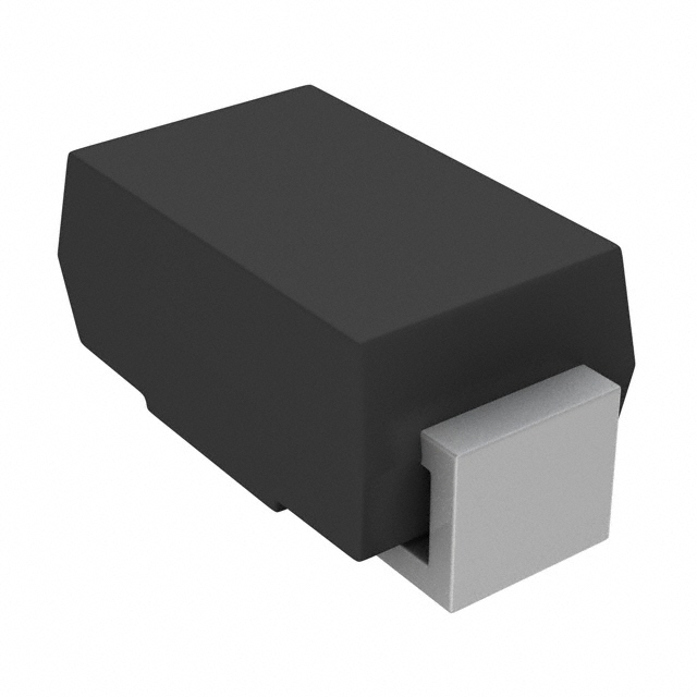
SMA (DO-214AC)
ADDITIONAL RESOURCES
• Base P/NHM3 - halogen-free, RoHS-compliant, and
AEC-Q101 qualified
3D 3D
• Material categorization: for definitions of compliance
please see www.vishay.com/doc?99912
3D Models
PRIMARY CHARACTERISTICS
PARAMETER
VZ range nom.
Test current IZT
VBR
VWM
PPPM
TJ max.
VZ specification
Circuit configuration
Polarity
VALUE
10 to 270
2 to 50
9.4 to 251
8.2 to 220
300
150
Pulse current
Single
Uni-directional
APPLICATIONS
UNIT
V
mA
V
V
W
°C
• Voltage stabilization
ORDERING INFORMATION
DEVICE NAME
BZG03C-M-series
BZG03C-M-series
BZG03C-M-series
BZG03C-M-series
ORDERING CODE
TAPED UNITS PER REEL
MINIMUM ORDER QUANTITY
BZG03Cxxx-M3-08
BZG03Cxxx-M3-18
BZG03Cxxx-HM3-08
BZG03Cxxx-HM3-18
1500 (7" reel)
6000 (13" reel)
1500 (7" reel)
6000 (13" reel)
6000/box
6000/box
6000/box
6000/box
MOISTURE SENSITIVITY
MSL level 1
(according J-STD-020)
SOLDERING CONDITIONS
PACKAGE
PACKAGE NAME
WEIGHT
MOLDING COMPOUND
SMA (DO-214AC)
73 mg
UL 94 V-0
Peak temperature max. 260 °C
ABSOLUTE MAXIMUM RATINGS (Tamb = 25 °C, unless otherwise specified)
PARAMETER
Power dissipation
Non repetitive peak surge power
Junction to lead
Junction to ambient air
Junction temperature
Storage temperature range
Operating temperature range
Forward voltage (max.)
TEST CONDITION
SYMBOL
VALUE
UNIT
RthJA < 25 K/W
RthJA < 100 K/W
tp = 100 μs sq.pulse, Tj = 25 °C prior to surge
Ptot
Ptot
PZSM
RthJL
RthJA
RthJA
RthJA
Tj
Tstg
Top
VF
3000
1250
600
25
150
125
100
150
-65 to +150
-65 to +150
1.2
mW
mW
W
K/W
K/W
K/W
K/W
°C
°C
°C
V
Mounted on epoxy-glass hard tissue, fig. 1a
Mounted on epoxy-glass hard tissue, fig. 1b
Mounted on Al-oxide-ceramic (Al2O3), fig. 1b
IF = 0.5 A
Rev. 1.2, 11-Sep-2019
Document Number: 86138
1
For technical questions within your region: DiodesAmericas@vishay.com, DiodesAsia@vishay.com, DiodesEurope@vishay.com
THIS DOCUMENT IS SUBJECT TO CHANGE WITHOUT NOTICE. THE PRODUCTS DESCRIBED HEREIN AND THIS DOCUMENT
ARE SUBJECT TO SPECIFIC DISCLAIMERS, SET FORTH AT www.vishay.com/doc?91000
�BZG03C-M-Series
www.vishay.com
Vishay Semiconductors
ELECTRICAL CHARACTERISTICS (Tamb = 25 °C, unless otherwise specified)
ZENER VOLTAGE
RANGE
TEST
CURRENT
VZ at IZT1
IZT1
V
mA
PART NUMBER
REVERSE
LEAKAGE
CURRENT
DYNAMIC
RESISTANCE
TEMPERATURE
COEFFICIENT OF ZENER
VOLTAGE
IR at VR
ZZ at IZT1
TKVZ at IZT1
μA
MIN.
NOM.
MAX.
BZG03C10-M
9.4
10
10.6
50
10
BZG03C11-M
10.4
11
11.6
50
BZG03C12-M
11.4
12
12.7
BZG03C13-M
12.4
13
14.1
BZG03C15-M
13.8
15
BZG03C16-M
15.3
16
BZG03C18-M
16.8
BZG03C20-M
18.8
BZG03C22-M
V
MAX.
%/K
TYP.
MAX.
MIN.
MAX.
7.5
2
4
0.05
0.09
4
8.2
4
7
0.05
0.1
50
3
9.1
4
7
0.05
0.1
50
2
10
5
10
0.05
0.1
15.6
50
1
11
5
10
0.05
0.1
17.1
25
1
12
6
15
0.06
0.11
18
19.1
25
1
13
6
15
0.06
0.11
20
21.2
25
1
15
6
15
0.06
0.11
20.8
22
23.3
25
1
16
6
15
0.06
0.11
BZG03C24-M
22.8
24
25.6
25
1
18
7
15
0.06
0.11
BZG03C27-M
25.1
27
28.9
25
1
20
7
15
0.06
0.11
BZG03C30-M
28
30
32
25
1
22
8
15
0.06
0.11
BZG03C33-M
31
33
35
25
1
24
8
15
0.06
0.11
BZG03C36-M
34
36
38
10
1
27
21
40
0.06
0.11
BZG03C39-M
37
39
41
10
1
30
21
40
0.06
0.11
BZG03C43-M
40
43
46
10
1
33
24
45
0.07
0.12
BZG03C47-M
44
47
50
10
1
36
24
45
0.07
0.12
BZG03C51-M
48
51
54
10
1
39
25
60
0.07
0.12
BZG03C56-M
52
56
60
10
1
43
25
60
0.07
0.12
BZG03C62-M
58
62
66
10
1
47
25
80
0.08
0.13
BZG03C68-M
64
68
72
10
1
51
25
80
0.08
0.13
BZG03C75-M
70
75
79
10
1
56
30
100
0.08
0.13
BZG03C82-M
77
82
87
10
1
62
30
100
0.08
0.13
BZG03C91-M
85
91
96
5
1
68
60
200
0.09
0.13
BZG03C100-M
94
100
106
5
1
75
60
200
0.09
0.13
BZG03C110-M
104
110
116
5
1
82
80
250
0.09
0.13
BZG03C120-M
114
120
127
5
1
91
80
250
0.09
0.13
BZG03C130-M
124
130
141
5
1
100
110
300
0.09
0.13
BZG03C150-M
138
150
156
5
1
110
130
300
0.09
0.13
BZG03C160-M
158
160
171
5
1
120
150
350
0.09
0.13
BZG03C180-M
168
180
191
5
1
130
180
400
0.09
0.13
BZG03C200-M
188
200
212
5
1
150
200
500
0.09
0.13
BZG03C220-M
208
220
233
2
1
160
350
750
0.09
0.13
BZG03C240-M
228
240
256
2
1
180
400
850
0.09
0.13
BZG03C270-M
251
270
289
2
1
200
450
1000
0.09
0.13
Rev. 1.2, 11-Sep-2019
Document Number: 86138
2
For technical questions within your region: DiodesAmericas@vishay.com, DiodesAsia@vishay.com, DiodesEurope@vishay.com
THIS DOCUMENT IS SUBJECT TO CHANGE WITHOUT NOTICE. THE PRODUCTS DESCRIBED HEREIN AND THIS DOCUMENT
ARE SUBJECT TO SPECIFIC DISCLAIMERS, SET FORTH AT www.vishay.com/doc?91000
�BZG03C-M-Series
www.vishay.com
Vishay Semiconductors
BASIC CHARACTERISTICS (Tamb = 25 °C, unless otherwise specified)
3.0
a)
b)
2
2.5
IF - Forward Current (A)
5
2
1.5
10
2.0
1.5
1.0
0.5
1
25
94 9313
0
0
25
0.5
10 000
3.5
3
RthJA = 25 K/W
2.5
2
1.5
RthJA = 100 K/W
1
0.5
0
0
25
50
75
100
125
1000
100
150
Tamb - Ambient Temperature (°C)
94 9580
10
0.01
0.1
1
10
tp - Pulse Length (ms)
94 9582
Fig. 2 - Total Power Dissipation vs. Ambient Temperature
Zthp - Thermal Resistance for Pulse Cond. (K/W)
2.0
1.5
Fig. 3 - Forward Current vs. Forward Voltage
PZSM - Non-Repetitive Surge Power
Dissipation (W)
Ptot - Total Power Dissipation (W)
Fig. 1 - Boards for RthJA Definition (Copper Overlay 35 µ)
1.0
VF - Forward Voltage (V)
94 9581
Fig. 4 - Non Repetitive Surge Power Dissipation vs.
Pulse Length
1000
100
tp/T = 0.5
10
tp/T = 0.2
tp/T = 0.1
tp/T = 0.05
tp/T = 0.02
1
10-5
94 9583
tp/T = 0.01
10-4
10-3
10-2
10-1
100
101
102
tp - Pulse Length (s)
Fig. 5 - Thermal Response
Rev. 1.2, 11-Sep-2019
Document Number: 86138
3
For technical questions within your region: DiodesAmericas@vishay.com, DiodesAsia@vishay.com, DiodesEurope@vishay.com
THIS DOCUMENT IS SUBJECT TO CHANGE WITHOUT NOTICE. THE PRODUCTS DESCRIBED HEREIN AND THIS DOCUMENT
ARE SUBJECT TO SPECIFIC DISCLAIMERS, SET FORTH AT www.vishay.com/doc?91000
�BZG03C-M-Series
www.vishay.com
Vishay Semiconductors
PACKAGE DIMENSIONS in millimeters (inches): SMA (DO-214AC)
5.5 (0.217)
4.9 (0.193)
4.5 (0.176)
0.1 (0.004)
0.2 (0.008)
2.0 (0.078)
2.3 (0.090)
4.2 (0.164)
3.3 (0.130)
2.8 (0.109)
2.3 (0.090)
1.4 (0.055)
1.7 (0.066)
2.5 (0.098)
Foot print recommendation:
2.21 (0.087)
2.3 (0.091) max.
Document no.: S8-V-3848.01-003 (4)
Created - Date: 18. February 1997
Rev. 8 - Date: 10. November 2006
2.2 (0.087) max.
6.7 (0.264) ref.
19628
Rev. 1.2, 11-Sep-2019
Document Number: 86138
4
For technical questions within your region: DiodesAmericas@vishay.com, DiodesAsia@vishay.com, DiodesEurope@vishay.com
THIS DOCUMENT IS SUBJECT TO CHANGE WITHOUT NOTICE. THE PRODUCTS DESCRIBED HEREIN AND THIS DOCUMENT
ARE SUBJECT TO SPECIFIC DISCLAIMERS, SET FORTH AT www.vishay.com/doc?91000
�Legal Disclaimer Notice
www.vishay.com
Vishay
Disclaimer
ALL PRODUCT, PRODUCT SPECIFICATIONS AND DATA ARE SUBJECT TO CHANGE WITHOUT NOTICE TO IMPROVE
RELIABILITY, FUNCTION OR DESIGN OR OTHERWISE.
Vishay Intertechnology, Inc., its affiliates, agents, and employees, and all persons acting on its or their behalf (collectively,
“Vishay”), disclaim any and all liability for any errors, inaccuracies or incompleteness contained in any datasheet or in any other
disclosure relating to any product.
Vishay makes no warranty, representation or guarantee regarding the suitability of the products for any particular purpose or
the continuing production of any product. To the maximum extent permitted by applicable law, Vishay disclaims (i) any and all
liability arising out of the application or use of any product, (ii) any and all liability, including without limitation special,
consequential or incidental damages, and (iii) any and all implied warranties, including warranties of fitness for particular
purpose, non-infringement and merchantability.
Statements regarding the suitability of products for certain types of applications are based on Vishay's knowledge of typical
requirements that are often placed on Vishay products in generic applications. Such statements are not binding statements
about the suitability of products for a particular application. It is the customer's responsibility to validate that a particular product
with the properties described in the product specification is suitable for use in a particular application. Parameters provided in
datasheets and / or specifications may vary in different applications and performance may vary over time. All operating
parameters, including typical parameters, must be validated for each customer application by the customer's technical experts.
Product specifications do not expand or otherwise modify Vishay's terms and conditions of purchase, including but not limited
to the warranty expressed therein.
Hyperlinks included in this datasheet may direct users to third-party websites. These links are provided as a convenience and
for informational purposes only. Inclusion of these hyperlinks does not constitute an endorsement or an approval by Vishay of
any of the products, services or opinions of the corporation, organization or individual associated with the third-party website.
Vishay disclaims any and all liability and bears no responsibility for the accuracy, legality or content of the third-party website
or for that of subsequent links.
Except as expressly indicated in writing, Vishay products are not designed for use in medical, life-saving, or life-sustaining
applications or for any other application in which the failure of the Vishay product could result in personal injury or death.
Customers using or selling Vishay products not expressly indicated for use in such applications do so at their own risk. Please
contact authorized Vishay personnel to obtain written terms and conditions regarding products designed for such applications.
No license, express or implied, by estoppel or otherwise, to any intellectual property rights is granted by this document or by
any conduct of Vishay. Product names and markings noted herein may be trademarks of their respective owners.
© 2024 VISHAY INTERTECHNOLOGY, INC. ALL RIGHTS RESERVED
Document Number: 91000
1
For technical questions, contact:
THIS DOCUMENT IS SUBJECT TO CHANGE WITHOUT NOTICE. THE PRODUCTS DESCRIBED HEREIN AND THIS DOCUMENT
ARE SUBJECT TO SPECIFIC DISCLAIMERS, SET FORTH AT www.vishay.com/doc?91000
Revision: 01-Jan-2024
�


 工商网监
湘ICP备2023018690号
工商网监
湘ICP备2023018690号
