DG2002
Vishay Siliconix
Low-Voltage Single SPDT Analog Switch
DESCRIPTION
FEATURES
The DG2002 is a single-pole/double-throw monolithic CMOS
analog switch designed for high performance switching of
analog signals. Combining low power, high speed (tON: 8 ns,
tOFF: 6 ns), low on-resistance (rDS(on): 7 Ω) and small
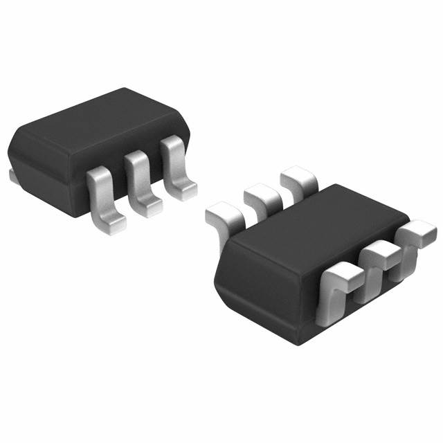
physical size (SC70), the DG2002 is ideal for portable and
battery powered applications requiring high performance
and efficient use of board space.
•
•
•
•
•
•
The DG2002 is built on Vishay Siliconix’s low voltage JI2
process. An epitaxial layer prevents latchup. Break-before make is guaranteed for DG2002.
BENEFITS
Each switch conducts equally well in both directions when
on, and blocks up to the power supply level when off.
Low voltage operation (1.8 V to 5.5 V)
Low on-resistance - rDS(on): 7 Ω
Fast switching - tON : 8 ns, tOFF: 6 ns
Low charge injection - QINJ: 5 pC
Low power consumption
TTL/CMOS compatible
• 6-pin SC70 package
•
•
•
•
Pb-free
Available
RoHS*
COMPLIANT
Reduced power consumption
Simple logic interface
High accuracy
Reduce board space
APPLICATIONS
•
•
•
•
•
Cellular phones
Communication systems
Portable test equipment
Battery operated systems
Sample and hold circuits
FUNCTIONAL BLOCK DIAGRAM AND PIN CONFIGURATION
TRUTH TABLE
SC-70
IN
1
6
NO (Source1)
V+
2
5
COM
GND
3
4
NC (Source2)
Top View
Logic
NC
NO
0
ON
OFF
1
OFF
ON
ORDERING INFORMATION
Temp Range
Package
- 40 to 85 °C
SC70-6
Device Marking: E2xx
Part Number
DG2002DL-T1
DG2002DL-T1-E3
* Pb containing terminations are not RoHS compliant, exemptions may apply.
Document Number: 71448
S-72609-Rev. C, 24-Dec-07
www.vishay.com
1
�DG2002
Vishay Siliconix
ABSOLUTE MAXIMUM RATINGS
Parameter
Referenced V+ to GND
IN, COM, NC, NOa
Limit
Unit
- 0.3 to +6
- 0.3 to (V+ + 0.3)
V
Continuous Current (Any Terminal)
± 50
Peak Current (Pulsed at 1 ms, 10 % duty cycle)
± 200
Storage Temperature
Power Dissipation (Packages)b
6-Pin SC70c
mA
- 65 to + 150
°C
250
mW
Notes:
a. Signals on NC, NO, or COM or IN exceeding V+ will be clamped by internal diodes. Limit forward diode current to maximum current ratings.
b. All leads welded or soldered to PC Board.
c. Derate 3.1 mW/°C above 70 °C.
SPECIFICATIONS V+ = 2.0 V
Parameter
Symbol
Test Conditions
Unless Otherwise Specified
V+ = 2.0 V, ± 10 %
VIN = 0.4 or 1.6 Ve
Limits
- 40 to 85 °C
Tempa
Minb
Full
0
Typc
Maxb
Unit
V+
V
Analog Switch
VNO, VNC
VCOM
Analog Signal Ranged
On-Resistance
rON Flatnessd
Switch Off Leakage Current
f
rON
V+ = 1.8 V, VCOM = 1.0 V, INO, INC = 10 mA
Room
Fulld
38
39.3
rON
Flatness
V+ = 1.8 V, VCOM = 0 to V+, INO, INC = 10 mA
Room
21
INO(off)
INC(off)
ICOM(off)
Channel-On Leakage
Currentf
ICOM(on)
V+ = 2.2 V
VNO, VNC = 0.5 V/1.5 V, VCOM = 1.5 V/0.5 V
V+ = 2.2 V, VNO, VNC = VCOM = 0.5 V/1.5 V
46.1
47.1
Ω
Room
Fulld
- 250
- 3.0
250
3.0
pA
nA
Room
Fulld
- 250
- 3.0
250
3.0
pA
nA
Room
Fulld
- 250
- 3.0
250
3.0
pA
nA
1.6
Digital Control
Input High Voltage
VINH
Full
Input Low Voltage
VINL
Full
Input Capacitanced
Cin
Input Current
IINL or IINH
0.4
Full
VIN = 0 or V+
Full
3
-1
V
pF
1
µA
Dynamic Characteristics
Turn-On Time
tON
Turn-Off Time
tOFF
Break-Before-Make Time
Charge Injectiond
d
Off-Isolation
d
Crosstalk
VNO or VNC = 1.5 V, RL = 300 Ω, CL = 35 pF
Figures 1 and 2
td
QINJ
OIRR
XTALK
NO, NC Off Capacitanced
CNO(off)
CNC(off)
Channel-On Capacitanced
CON
Room
Fulld
22
31
32
Room
Fulld
10
17
18
ns
10
pC
Room
CL = 1 nF, VGEN = 0 V, RGEN = 0 Ω, Figure 3
RL = 50 Ω, CL = 5 pF, f = 1 MHz
VIN = 0 or V+, f = 1 MHz
1
12
Room
5
Room
- 67
Room
- 71
Room
5
Room
29
dB
pF
Power Supply
Power Supply Range
V+
Power Supply Currentd
I+
Power Consumption
PC
www.vishay.com
2
1.8
VIN = 0 or V+
0.01
2.2
V
1.0
µA
2.2
µW
Document Number: 71448
S-72609-Rev. C, 24-Dec-07
�DG2002
Vishay Siliconix
SPECIFICATIONS V+ = 3.0 V
Parameter
Symbol
Test Conditions
Unless Otherwise Specified
V+ = 3 V, ±10 %
VIN = 0.4 or 2.0 Ve
Limits
- 40 to 85 °C
Tempa
Minb
Full
0
Typc
Maxb
Unit
V+
V
Analog Switch
VNO, VNC
VCOM
Analog Signal Ranged
On-Resistanced
rON Flatnessd
Switch Off Leakage Current
f
rON
V+ = 2.7 V, VCOM = 1.5 V, INO, INC = 10 mA
Room
Full
12.2
13
rON
Flatness
V+ = 2.7 V, VCOM = 0 to V+, INO, INC = 10 mA
Room
5
INO(off)
INC(off)
ICOM(off)
Channel-On Leakage
Currentf
ICOM(on)
V+ = 3.3 V
VNO, VNC = 1 V/3 V, VCOM = 3 V/1 V
V+ = 3.3 V, VNO, VNC = VCOM = 1 V/3 V
14.8
15.8
Ω
Room
Full
- 500
- 4.0
500
4.0
pA
nA
Room
Full
- 500
- 4.0
500
4.0
pA
nA
Room
Full
- 500
- 4.0
500
4.0
pA
nA
2
Digital Control
Input High Voltage
VINH
Full
Input Low Voltage
VINL
Full
Input Capacitanced
Cin
IINL or IINH
Input Current
0.4
Full
VIN = 0 or V+
Full
3
-1
V
pF
1
µA
Dynamic Characteristics
Turn-On Timed
tON
Turn-Off Timed
tOFF
Break-Before-Make Timed
Charge Injection
Off-Isolation
d
d
Crosstalkd
VNO or VNC = 2.0 V, RL = 300 Ω, CL = 35 pF
Figures 1 and 2
td
QINJ
OIRR
XTALK
NO, NC Off Capacitanced
CNO(off)
CNC(off)
Channel-On Capacitanced
CON
Room
Full
12
21
22
Room
Full
7
14
15
ns
10
pC
Room
CL = 1 nF, VGEN = 0 V, RGEN = 0 Ω, Figure 3
RL = 50 Ω, CL = 5 pF, f = 1 MHz
VIN = 0 or V+, f = 1 MHz
1
6
Room
5
Room
- 67
Room
- 69
Room
5
Room
29
dB
pF
Power Supply
Power Supply Range
V+
Power Supply Current
I+
Power Consumption
PC
Document Number: 71448
S-72609-Rev. C, 24-Dec-07
2.7
VIN = 0 or V+
0.01
3.3
V
1.0
µA
3.3
µW
www.vishay.com
3
�DG2002
Vishay Siliconix
SPECIFICATIONS V+ = 5.0 V
Parameter
Symbol
Test Conditions
Unless Otherwise Specified
V+ = 5 V, ± 10 %
VIN = 0.8 or 2.4 Ve
Limits
- 40 to 85 °C
Tempa
Minb
Full
0
Typc
Maxb
Unit
V+
V
Analog Switch
Analog Signal Ranged
On-Resistance
rON Flatnessd
Switch Off Leakage Current
VNO, VNC,
VCOM
rON
V+ = 4.5 V, VCOM = 3 V, INO, INC = 10 mA
Room
Full
6.4
7.4
rON
Flatness
V+ = 4.5 V, VCOM = 0 to V+, INO, INC = 10 mA
Room
3
INO(off),
INC(off)
ICOM(off)
Channel-On Leakage Current
ICOM(on)
V+ = 5.5 V
VNO, VNC = 1 V/4.5 V, VCOM = 4.5 V/1 V
V+ = 5.5 V, V+ = 5.5 V
VNO, VNC = VCOM = 1 V/4.5 V
7.8
8.8
Room
Full
- 1.0
- 4.0
1.0
4.0
Room
Full
- 1.0
- 4.0
1.0
4.0
Room
Full
- 1.0
- 4.0
1.0
4.0
2.4
Ω
nA
Digital Control
Input High Voltage
VINH
Full
Input Low Voltage
VINL
Full
Input Capacitance
Cin
IINL or IINH
Input Current
0.8
Full
VIN = 0 or V+
Full
3
-1
V
pF
1
µA
Dynamic Characteristics
Turn-On Timed
tON
Turn-Off Timed
tOFF
Break-Before-Make Timed
Charge Injection
d
VNO or VNC = 3 V, RL = 300 Ω, CL = 35 pF
Figures 1 and 2
td
QINJ
Off-Isolationd
OIRR
Crosstalkd
XTALK
Source-Off Capacitanced
CNO(off),
CNC(off)
Channel-On Capacitanced
CON
Room
Full
8
15
16
Room
Full
6
13
14
ns
10
pC
Room
CL = 1 nF, VGEN = 0 V, RGEN = 0 Ω, Figure 3
RL = 50 Ω, CL = 5 pF, f = 1 MHz
VIN = 0 or V+, f = 1 MHz
1
4
Room
5
Room
- 69
Room
- 69
Room
5
Room
29
dB
pF
Power Supply
Power Supply Range
V+
Power Supply Current
I+
Power Consumption
PC
4.5
VIN = 0 or V+
0.01
5.5
V
1.0
µA
5.5
µW
Notes:
a. Room = 25 °C, Full = as determined by the operating suffix.
b. The algebraic convention whereby the most negative value is a minimum and the most positive a maximum, is used in this data sheet.
c. Typical values are for design aid only, not guaranteed nor subject to production testing.
d. Guarantee by design, nor subjected to production test.
e. VIN = input voltage to perform proper function.
f. Guaranteed by 5 V leakage testing, not production tested.
Stresses beyond those listed under “Absolute Maximum Ratings” may cause permanent damage to the device. These are stress ratings only, and functional operation
of the device at these or any other conditions beyond those indicated in the operational sections of the specifications is not implied. Exposure to absolute maximum
rating conditions for extended periods may affect device reliability.
www.vishay.com
4
Document Number: 71448
S-72609-Rev. C, 24-Dec-07
�DG2002
Vishay Siliconix
TYPICAL CHARACTERISTICS 25 °C, unless otherwise noted
40
35
35
30
r ON - On-Resistance (Ω)
r ON - On-Resistance (Ω)
V+ = 1.8 V
30
25
20
V+ = 2 V
15
V+ = 3 V
V+ = 5 V
10
25
V+ = 2 V
20
85 °C
15
25 °C
- 40 °C
85 °C
25 °C
- 40 °C
10
5
5
0
0
0
1
2
3
4
5
0
1
2
VCOM - Analog Voltage (V)
3
4
5
6
VCOM - Analog Voltage (V)
rON vs. VCOM and Supply Voltage
rON vs. Analog Voltage and Temperature
10
10 m
V+ = 5 V
VIN = 0 V
1m
I+ - Supply Current (A)
I+ - Supply Current (nA)
V+ = 5 V
1
0.1
100 µ
10 µ
1µ
100 n
10 n
0.01
- 60
1n
- 40
- 20
0
20
40
60
80
100
10
100 K
1M
10 M
Supply Current vs. Input Switching Frequency
150
V+ = 5 V
T = 25 °C
100
Leakage Current (pA)
1000
Leakage Current (pA)
10 K
Supply Current vs. Temperature
V+ = 5 V
INO(off)/INC(off)
10
50
0
ICOM(off)
INO(off)/INC(off)
- 50
ICOM(on)
ICOM(on)
- 100
ICOM(off)
1
- 60
1K
Input Switching Frequency (Hz)
10000
100
100
Temperature (°C)
- 150
- 40
- 20
0
20
40
60
Temperature (°C)
Leakage Current vs. Temperature
Document Number: 71448
S-72609-Rev. C, 24-Dec-07
80
100
0
1
2
3
4
5
VCOM, V NO, V NC - Analog Voltage
Leakage vs. Analog Voltage
www.vishay.com
5
�DG2002
Vishay Siliconix
TYPICAL CHARACTERISTICS 25 °C, unless otherwise noted
30
0
Loss, OIRR, XTALK (dB)
t ON, t OFF - Switching Time (ns)
tON V+ = 2 V
25
20
tON V+ = 3 V
15
tON V+ = 5 V
tOFF V+ = 2 V
10
tOFF V+ = 3 V
5
- 40
- 20
0
20
40
60
80
- 20
- 30
- 40
- 50
OIRR
- 60
XTALK
- 90
- 100
100 K
100
1M
Temperature (°C)
10 M
100 M
1G
Frequency (Hz)
Switching Time vs. Temperature
and Supply Voltage
Insertion Loss, Off -Isolation
Crosstalk vs. Frequency
1.8
20
1.6
15
1.4
Q - Charge Injection (pC)
V T - Switching Threshold (V)
V+ = 3 V
RL = 50 Ω
- 70
- 80
tOFF V+ = 5 V
0
- 60
LOSS
- 10
1.2
1.0
0.8
0.6
0.4
10
V+ = 5 V
5
0
V+ = 3 V
-5
V+ = 2 V
V+ = 2.5 V
- 10
- 15
0.2
0.0
- 20
0
www.vishay.com
6
1
2
3
4
5
6
0
1
2
3
4
5
V+ - Supply Voltage (V)
VCOM - Analog Voltage (V)
Switching Threshold vs. Supply Voltage
Charge Injection vs. Analog Voltage
6
Document Number: 71448
S-72609-Rev. C, 24-Dec-07
�DG2002
Vishay Siliconix
TEST CIRCUITS
V+
VINH
Logic
Input
VINL
V+
Switch
Input
Switch Output
COM
NO or NC
tr < 5 ns
tf < 5 ns
50 %
VOUT
0.9 x VOUT
Switch
Output
IN
Logic
Input
RL
300 Ω
GND
CL
35 pF
0V
tOFF
tON
Logic "1" = Switch On
Logic input waveforms inverted for switches that have
the opposite logic sense.
CL (includes fixture and stray capacitance)
RL
VOUT = VCOM
R L + R ON
Figure 1. Switching Time
V+
Logic
Input
V+
tr < 5 ns
tf < 5 ns
VINL
COM
NO
VNO
VINH
VO
NC
VNC
RL
300 Ω
IN
CL
35 pF
VNC = VNO
VO
GND
Switch
Output
90 %
0V
tD
tD
CL (includes fixture and stray capacitance)
Figure 2. Break-Before-Make Interval
V+
Rgen
ΔVOUT
V+
COM
NC or NO
VOUT
VOUT
+
Vgen
IN
CL = 1 nF
IN
On
Off
On
GND
Q = ΔVOUT x CL
VIN = 0 - V+
IN depends on switch configuration: input polarity
determined by sense of switch.
Figure 3. Charge Injection
Document Number: 71448
S-72609-Rev. C, 24-Dec-07
www.vishay.com
7
�DG2002
Vishay Siliconix
TEST CIRCUITS
V+
10 nF
V+
NC or NO
0V, 2.4 V
IN
COM
RL
V COM
Off Isolation = 20 log V
NO/ NC
GND
Analyzer
Figure 4. Off-Isolation
V+
10 nF
V+
COM
Meter
IN
0 V, 2.4 V
NC or NO
GND
HP4192A
Impedance
Analyzer
or Equivalent
f = 1 MHz
Figure 5. Channel Off/On Capacitance
Vishay Siliconix maintains worldwide manufacturing capability. Products may be manufactured at one of several qualified locations. Reliability data for Silicon
Technology and Package Reliability represent a composite of all qualified locations. For related documents such as package/tape drawings, part marking, and
reliability data, see http://www.vishay.com/ppg?71448.
www.vishay.com
8
Document Number: 71448
S-72609-Rev. C, 24-Dec-07
�Package Information
Vishay Siliconix
SCĆ70:
6ĆLEADS
MILLIMETERS
6
5
Dim
A
A1
A2
b
c
D
E
E1
e
e1
L
4
E1 E
1
2
3
-B-
e
b
e1
D
-Ac
A2 A
L
A1
Document Number: 71154
06-Jul-01
INCHES
Min
Nom
Max
Min
Nom
Max
0.90
–
1.10
0.035
–
0.043
–
–
0.10
–
–
0.004
0.80
–
1.00
0.031
–
0.039
0.15
–
0.30
0.006
–
0.012
0.10
–
0.25
0.004
–
0.010
1.80
2.00
2.20
0.071
0.079
0.087
1.80
2.10
2.40
0.071
0.083
0.094
1.15
1.25
1.35
0.045
0.049
0.053
0.65BSC
0.026BSC
1.20
1.30
1.40
0.047
0.051
0.055
0.10
0.20
0.30
0.004
0.008
0.012
7_Nom
7_Nom
ECN: S-03946—Rev. B, 09-Jul-01
DWG: 5550
www.vishay.com
1
�Legal Disclaimer Notice
www.vishay.com
Vishay
Disclaimer
ALL PRODUCT, PRODUCT SPECIFICATIONS AND DATA ARE SUBJECT TO CHANGE WITHOUT NOTICE TO IMPROVE
RELIABILITY, FUNCTION OR DESIGN OR OTHERWISE.
Vishay Intertechnology, Inc., its affiliates, agents, and employees, and all persons acting on its or their behalf (collectively,
“Vishay”), disclaim any and all liability for any errors, inaccuracies or incompleteness contained in any datasheet or in any other
disclosure relating to any product.
Vishay makes no warranty, representation or guarantee regarding the suitability of the products for any particular purpose or
the continuing production of any product. To the maximum extent permitted by applicable law, Vishay disclaims (i) any and all
liability arising out of the application or use of any product, (ii) any and all liability, including without limitation special,
consequential or incidental damages, and (iii) any and all implied warranties, including warranties of fitness for particular
purpose, non-infringement and merchantability.
Statements regarding the suitability of products for certain types of applications are based on Vishay's knowledge of typical
requirements that are often placed on Vishay products in generic applications. Such statements are not binding statements
about the suitability of products for a particular application. It is the customer's responsibility to validate that a particular product
with the properties described in the product specification is suitable for use in a particular application. Parameters provided in
datasheets and / or specifications may vary in different applications and performance may vary over time. All operating
parameters, including typical parameters, must be validated for each customer application by the customer's technical experts.
Product specifications do not expand or otherwise modify Vishay's terms and conditions of purchase, including but not limited
to the warranty expressed therein.
Hyperlinks included in this datasheet may direct users to third-party websites. These links are provided as a convenience and
for informational purposes only. Inclusion of these hyperlinks does not constitute an endorsement or an approval by Vishay of
any of the products, services or opinions of the corporation, organization or individual associated with the third-party website.
Vishay disclaims any and all liability and bears no responsibility for the accuracy, legality or content of the third-party website
or for that of subsequent links.
Except as expressly indicated in writing, Vishay products are not designed for use in medical, life-saving, or life-sustaining
applications or for any other application in which the failure of the Vishay product could result in personal injury or death.
Customers using or selling Vishay products not expressly indicated for use in such applications do so at their own risk. Please
contact authorized Vishay personnel to obtain written terms and conditions regarding products designed for such applications.
No license, express or implied, by estoppel or otherwise, to any intellectual property rights is granted by this document or by
any conduct of Vishay. Product names and markings noted herein may be trademarks of their respective owners.
© 2022 VISHAY INTERTECHNOLOGY, INC. ALL RIGHTS RESERVED
Revision: 01-Jan-2022
1
Document Number: 91000
�