DG200A_MIL
Vishay Siliconix
Monolithic Dual SPST CMOS Analog Switch
FEATURES
BENEFITS
APPLICATIONS
D
D
D
D
D Wide Dynamic Range
D Simple Interfacing
D Reduced External Component
Count
D
D
D
D
"15 V Input Signal Range
44-V Maximum Supply Ranges
On-Resistance: 45 W
TTL and CMOS Compatibility
Servo Control Switching
Programmable Gain Amplifiers
Audio Switching
Programmable Filters
DESCRIPTION
The DG200A_MIL is a dual, single-pole, single-throw analog
switch designed to provide general purpose switching of
analog signals. This device is ideally suited for designs
requiring a wide analog voltage range coupled with low
on-resistance.
Each switch conducts equally well in both directions when on,
and blocks up to 30 V peak-to-peak when off. In the on
condition, this bi-directional switch introduces no offset
voltage of its own.
The DG200A_MIL is designed on Vishay Siliconix’ improved
PLUS-40 CMOS process. An epitaxial layer prevents latchup.
FUNCTIONAL BLOCK DIAGRAM AND PIN CONFIGURATION
Dual-In-Line
Metal Can
IN2
IN1
1
14
NC
2
13
NC
V+ (Substrate and Case)
IN1
GND
3
12
V+ Substrate
NC
4
11
NC
S2
5
10
S1
D2
6
9
D1
V–
8
7
1
IN2
GND
S1
9
2
8
7
3
4
NC
10
S2
D1
NC
6
5
V–
D2
Top View
Top View
TRUTH TABLE
Logic
Switch
0
ON
1
OFF
Logic “0” v 0.8 V
Logic “1” w 2.4 V
Document Number: 70035
S-02314—Rev. E, 05-Oct-00
www.vishay.com
4-1
�DG200A_MIL
Vishay Siliconix
ORDERING INFORMATION
Temp Range
Package
Part Number
DG200AAK
14-Pin CerDIP
–55 to 125_C
DG200AAK/883, JM38510/12301BCA,
5962-9562901QCA
DG200AAA
10-Pin Metal Can
14-Pin Sidebraze
DG200AAA/883, JM38510/12301BIC
JM38510/12301BCC
ABSOLUTE MAXIMUM RATINGS
V+ to V– . . . . . . . . . . . . . . . . . . . . . . . . . . . . . . . . . . . . . . . . . . . . . . . . . . . . . . 44 V
GND to V– . . . . . . . . . . . . . . . . . . . . . . . . . . . . . . . . . . . . . . . . . . . . . . . . . . . . 25 V
Digital Inputsa, VS, VD . . . . . . . . . . . . . . . . . . . . . . . . (V–) –2 V to (V+) +2 V or
30 mA, whichever occurs first
Current (Any Terminal) Continuous . . . . . . . . . . . . . . . . . . . . . . . . . . . . . 30 mA
Current S or D
(Pulsed at 1 ms, 10% Duty Cycle Max) . . . . . . . . . . . . . . . . . . . . . . . . . 100 mA
Storage Temperature . . . . . . . . . . . . . . . . . . . . . . . . . . . . . . . . . . . –65 to 150_C
Power Dissipation (Package)b
10-Pin Metal Canc . . . . . . . . . . . . . . . . . . . . . . . . . . . . . . . . . . . . . . . . . . 450 mW
14-Pin CerDIPd . . . . . . . . . . . . . . . . . . . . . . . . . . . . . . . . . . . . . . . . . . . . 825 mW
Notes:
a. Signals on SX, DX, or INX exceeding V+ or V– will be clamped by internal
diodes. Limit forward diode current to maximum current ratings.
b. All leads welded or soldered to PC Board.
c. Derate 6 mW/_C above 75_C
d. Derate 11 mW/_C above 75_C
SCHEMATIC DIAGRAM (TYPICAL CHANNEL)
V+
S
V–
–
+
V+
GND
INX
D
V–
FIGURE 1.
www.vishay.com
4-2
Document Number: 70035
S-02314—Rev. E, 05-Oct-00
�DG200A_MIL
Vishay Siliconix
SPECIFICATIONSa
Limits
Test Conditions
Unless Otherwise Specified
Parameter
Symbol
V+ = 15 V, V– = –15 V
VIN = 2.4 V, 0.8 Vf
–55 to 125_C
Tempb
Minc
Full
–15
Typd
Maxc
Unit
15
V
45
70
100
W
Analog Switch
Analog Signal Rangee
Drain-Source
On-Resistance
VANALOG
rDS(on)
VD = "10 V, IS = –1 mA
Room
Full
Source Off
Leakage Current
IS(off)
VS = "14 V, VD = #14 V
Room
Full
–2
–100
"0.01
2
100
Drain Off
Leakage Current
ID(off)
VD = "14 V, VS = #14 V
Room
Full
–2
–100
"0.01
2
100
Channel On
Leakage Currentf
ID(on)
VS = VD = "14 V
Room
Full
–2
–200
"0.1
2
200
VIN = 2.4 V
Room
Full
–0.5
–1
0.0009
VIN = 15 V
Room
Full
VIN = 0 V
Room
Full
nA
Digital Control
Input Current with
Input Voltage High
IINH
Input Current with
Input Voltage Low
IINL
0.005
–0.5
–1
0.5
1
mA
–0.0015
Dynamic Characteristics
Turn-On Time
Turn-Off Time
Charge Injection
Source-Off Capacitance
Drain-Off Capacitance
Channel-On Capacitance
Off Isolation
Crosstalk
(Channel-to-Channel)
tON
tOFF
Q
CS(off)
CD(off)
CD(on) +
CS(On)
Room
440
1000
Room
340
425
Room
–10
VS = 0 V
Room
9
VD = 0 V
Room
9
Room
25
Room
75
Room
90
Room
0.8
See Switching Time Test Circuit
CL = 1000 pF, Vg = 0 V
Rg = 0 W
f = 140 kHz
VIN = 5 V
VD = VS = 0 V, VIN = 0 V
OIRR
XTALK
VIN = 5 V, RL = 75 W
VS = 2 V, f = 1 MHz
ns
pC
pF
dB
Power Supplies
Positive Supply Current
I+
Negative Supply Current
I–
Both Channels On or Off
VIN = 0 V and 2.4 V
2
mA
Room
–1
–0.23
Notes:
a. Refer to PROCESS OPTION FLOWCHART.
b. Room = 25_C, Full = as determined by the operating temperature suffix.
c. The algebraic convention whereby the most negative value is aminimum and the most positive a maximum, is used in this data sheet.
d. Typical values are for DESIGN AID ONLY, not guaranteed nor subject to production testing.
e. Guaranteed by design, not subject to production test.
f.
VIN = input voltage to perform proper function.
Document Number: 70035
S-02314—Rev. E, 05-Oct-00
www.vishay.com
4-3
�DG200A_MIL
Vishay Siliconix
TYPICAL CHARACTERISTICS (25_C UNLESS NOTED)
rDS(on) vs. VD and Power Supply Voltage
Leakage Currents vs. Analog Voltage
+6
TA = 25_C
ID(off) or IS(off)
0
A
I S, I D (pA)
100
r DS(on) ( W )
"5 V
"10 V
"12 V
"15 V
"20 V
A:
B:
C:
D:
E:
120
80
B
60
ID(on)
–6
–12
C
D
40
–18
E
–24
20
–15 –12
–9
–6
–3
0
3
6
9
12
–15 –12
15
VD – Drain Voltage (V)
V T (V)
1.5
1.0
0.5
0
0
"5
"10
"15
V+, V– Positive and Negative Supplies (V)
www.vishay.com
4-4
–3
0
3
6
9
12
15
"20
Supply Currents vs. Toggle Frequency
V+ = 15 V
V– = –15 V
Both logic inputs
toggled simutaneously
6
5
I+, I– (mA)
ÉÉÉÉÉÉÉÉÉ
ÉÉÉÉÉÉÉÉÉ
ÉÉÉÉÉÉÉÉÉ
ÉÉÉÉÉÉÉÉÉ
ÉÉÉÉÉÉÉÉÉ
ÉÉÉÉÉÉÉÉÉ
ÉÉÉÉÉÉÉÉÉ
ÉÉÉÉÉÉÉÉÉ
ÉÉÉÉÉÉÉÉÉ
2.0
–6
VANALOG – Analog Voltage (V)
Input Switching Threshold vs. V+ and V– Supply Voltages
2.5
–9
4
3
2
I+
1
I–
0
1k
10 k
100 k
1M
Toggle Frequency (Hz)
Document Number: 70035
S-02314—Rev. E, 05-Oct-00
�DG200A_MIL
Vishay Siliconix
TEST CIRCUITS
VO is the steady state output with switch on. Feedthrough via gate capacitance may result in spikes at leading and trailing edge of output waveform.
+15 V
Logic
Input
Switch
Input
3V
V+
tr
很抱歉,暂时无法提供与“DG200AAK”相匹配的价格&库存,您可以联系我们找货
免费人工找货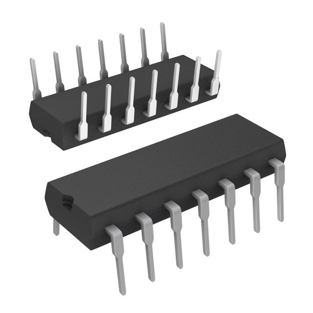


 工商网监
湘ICP备2023018690号
工商网监
湘ICP备2023018690号
