DG2011
Vishay Siliconix
Low-Voltage, Low rON, Single SPDT Analog Switch
In SC-89 Package
DESCRIPTION
FEATURES
The DG2011 is a low on-resistance, single-pole/doublethrow monolithic CMOS analog switch. It is designed for low
voltage applications with guaranteed operation at 2 V. The
DG2011 is ideal for portable and battery powered equipment,
requiring high performance and efficient use of board space.
In additional to the low on-resistance (1.8 Ω at 2.7 V), charge
injection is less than 10 pC over the entire analog range.
•
•
•
•
•
The switch conducts equally well in both directions when on,
and blocks up to the power supply level when off.
The DG2011 is built on Vishay Siliconix’s low voltage JI2 process. An epitaxial layer prevents latchup.
Break-before-make is guaranteed.
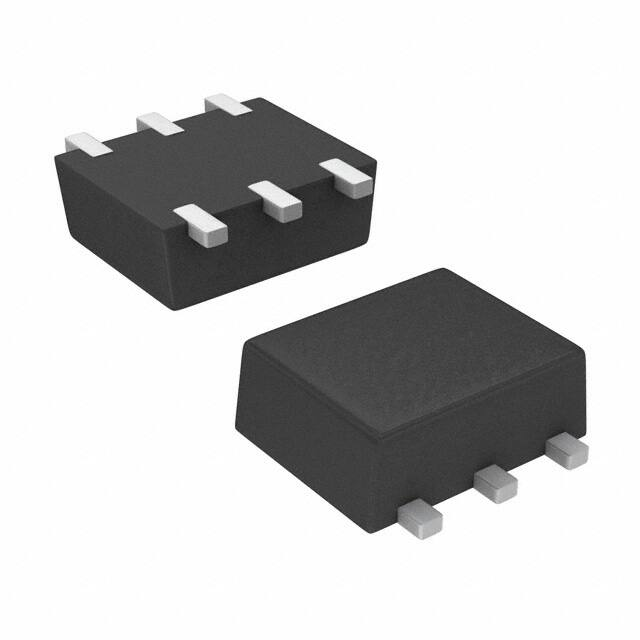
The DG2011 represents a breakthrough in packaging development for analog switching products. The SC-89 package
(1.6 x 1.6 mm2) – also know as SOT-666 in the industry –
reduces board spacing by approximately 40 % while obtaining performance comparable to SC-70 analog switch devices
available today.
As a committed partner to the community and the environment, Vishay Siliconix manufactures this product with the
lead (Pb)-free device terminations. For analog switching
products manufactured with 100 % matte tin device terminations, the lead (Pb)-free “-E3” suffix is being used as a designator.
Low Voltage Operation (1.8 V to 5.5 V)
Low On-Resistance - rON: 1.8 Ω at 2.7 V
Low Charge Injection
Low Voltage Logic Compatible
SC-89 Package (1.6 x 1.6 mm)
Pb-free
Available
RoHS*
COMPLIANT
BENEFITS
•
•
•
•
•
Reduced Power Consumption
Simple Logic Interface
High Accuracy
Reduce Board Space
Guaranteed 2 V Operation
APPLICATIONS
•
•
•
•
•
•
•
Cellular Phones
Communication Systems
Portable Test Equipment
Battery Operated Systems
Sample and Hold Circuits
ADC and DAC Applications
Low Voltage Data Acquisition Systems
FUNCTIONAL BLOCK DIAGRAM AND PIN CONFIGURATION
TRUTH TABLE
SC-89
IN
1
6
NO (Source1)
V+
2
5
COM
GND
3
4
NC (Source2)
Top View
Logic
NC
NO
0
ON
OFF
1
OFF
ON
COMMERCIAL ORDERING INFORMATION
Temp Range
Ax
- 40 to 85 °C
Pin 1
Device Marking: Ax
x = Date/Lot Traceability Code
Package
Part Number
SC-89 (SOT-666)
with Tape and Reel
DG2011DX-T1**
SC-89 (SOT-666)
Lead (Pb)-free
with Tape and Reel
DG2011DX-T1-E3**
DG2011DXA-T1-E3
** Note:
DG2011DX-T1 and DG2011DX-T1-E3 are not recommended for
new designs.
* Pb containing terminations are not RoHS compliant, exemptions may apply.
Document Number: 70102
S-60004–Rev. F, 16-Jan-06
www.vishay.com
1
�DG2011
Vishay Siliconix
ABSOLUTE MAXIMUM RATINGS TA = 25 °C, unless otherwise noted
Parameter
Symbol
Limit
Reference V+ to GND
Unit
- 0.3 to + 6
V
- 0.3 to (V+ + 0.3 V)
IN, COM, NC, NOa
Continuous Current (NO, NC, COM pins)
± 150
Peak Current (Pulsed at 1 ms, 10 % duty cycle)
± 300
mA
Storage Temperature
D Suffix
- 65 to 150
°C
Power Dissipation (Packages)b
SC-89c
172
mW
Notes:
a. Signals on NC, NO, or COM or IN exceeding V+ will be clamped by internal diodes. Limit forward diode current to maximum current ratings.
b. All leads welded or soldered to PC Board.
c. Derate 2.15 mW/°C above 70 °C.
SPECIFICATIONS (V+ = 2.0 V)
Test Conditions
Otherwise Unless Specified
Parameter
Analog Switch
Analog Signal Ranged
On-Resistance
Switch Off Leakage Currentf
Symbol
VNO, VNC,
VCOM
rON
INO(off)
INC(off)
ICOM(off)
Channel-On Leakage Currentf
V+ = 2.0 V, VIN = 0.4 V or 1.6 Ve
ICOM(on)
V+ = 2.0 V, VCOM = 0.2 V/0.9 V
INO, INC = 20 mA
V+ = 2.2 V,
VNO, VNC= 0.5 V/1.5 V, VCOM = 1.5 V/0.5 V
V+ = 2.2 V, VNO, VNC = VCOM = 0.5 V/1.5 V
Limits
- 40 to 85 °C
Tempa
Minb
Full
0
Typc
3.5
Room
Full
Maxb
Unit
V+
V
5.5
5.5
Ω
Room
Full
-1
- 10
1
10
Room
Full
Room
Full
-1
- 10
-1
- 10
1
10
1
10
1.5
nA
Digital Control
Input High Voltage
VINH
Full
Input Low Voltage
VINL
Full
Input Capacitance
Input Current
Dynamic Characteristics
Cin
IINL or IINH
Turn-On Time
tON
Turn-Off Time
tOFF
Break-Before-Make Time
tBBM
Charge Injectiond
QINJ
Off-Isolationd
OIRR
Crosstalkd
XTALK
NO, NC Off Capacitanced
Channel-On Capacitanced
Power Supply
CNO(off)
CNC(off)
V+
Negative Supply Current
I+
www.vishay.com
2
4
Full
VIN = 0 or V+
Full
VNO or VNC = 1.5 V, RL = 300 Ω, CL = 35 pF
Room
Full
Room
Full
Room
CL = 1 nF, VGEN = 0 V, RGEN = 0 Ω
Room
7
Room
- 62
Room
- 69
Room
29
Room
85
RL = 50 Ω, CL = 5 pF, f = 1 MHz
VIN = 0 or V+, f = 1 MHz
CON
Positive Supply Range
0.4
VIN = 0 or V+
1
37
1
pF
1
75
V
110
113
71
76
µA
ns
37
1.8
pC
dB
pF
5.5
0.01
1.0
V
µA
Document Number: 70102
S-60004–Rev. F, 16-Jan-06
�DG2011
Vishay Siliconix
SPECIFICATIONS (V+ = 3 V)
Test Conditions
Otherwise Unless Specified
Parameter
Analog Switch
Analog Signal Ranged
On-Resistance
rON Match
rON Flatness
Switch Off Leakage Current
Symbol
VNO, VNC,
VCOM
rON
ΔrON
rON
Flatness
INO(off)
INC(off)
ICOM(off)
Channel-On Leakage Currentf
V+ = 3 V, ±10 %,VIN = 0.4 V or 2.0 Ve
ICOM(on)
V+ = 2.7 V, VCOM = 0.9 V/1.5 V
INO, INC = 50 mA
V+ = 3.3 V,
VNO, VNC= 1 V/3 V, VCOM = 3 V/1 V
V+ = 3.3 V, VNO, VNC = VCOM = 1 V/3 V
Limits
–40 to 85 °C
Tempa
Minb
Full
0
Typc
Room
Full
Room
1.8
Room
0.2
Maxb
Unit
V+
V
2.7
2.9
0.2
Ω
0.5
Room
Full
-1
- 10
1
10
Room
Full
Room
Full
-1
- 10
-1
- 10
1
10
1
10
1.6
nA
Digital Control
Input High Voltage
VINH
Full
Input Low Voltage
VINL
Full
Input Capacitance
Input Current
Dynamic Characteristics
Cin
IINL or IINH
Turn-On Time
tON
Turn-Off Time
tOFF
Break-Before-Make Time
tBBM
Charge Injectiond
QINJ
Off-Isolationd
OIRR
Crosstalkd
XTALK
NO, NC Off Capacitanced
Channel-On Capacitanced
Power Supply
CNO(off)
CNC(off)
V+
Power Supply Current
I+
Power Consumption
PC
4
Full
VIN = 0 or V+
Full
VNO or VNC = 2.0 V, RL = 300 Ω, CL = 35 pF
Room
Full
Room
Full
Room
CL = 1 nF, VGEN = 0 V, RGEN = 0 Ω
Room
2
Room
- 62
Room
- 68
Room
28
Room
84
RL = 50 Ω, CL = 5 pF, f = 1 MHz
VIN = 0 or V+, f = 1 MHz
CON
Power Supply Range
0.4
1
29
1
75
77
59
62
µA
ns
16
1.8
VIN = 0 or V+
pF
1
45
V
pC
dB
pF
5.5
0.01
1.0
V
µA
3.3
µW
Notes:
a. Room = 25 °C, Full = as determined by the operating suffix.
b. Typical values are for design aid only, not guaranteed nor subject to production testing.
c. The algebraic convention whereby the most negative value is a minimum and the most positive a maximum, is used in this data sheet.
d. Guarantee by design, nor subjected to production test.
e. VIN = input voltage to perform proper function.
f. Guaranteed by 5 V leakage testing, not production tested.
Stresses beyond those listed under “Absolute Maximum Ratings” may cause permanent damage to the device. These are stress ratings only, and functional operation
of the device at these or any other conditions beyond those indicated in the operational sections of the specifications is not implied. Exposure to absolute maximum
rating conditions for extended periods may affect device reliability.
Document Number: 70102
S-60004–Rev. F, 16-Jan-06
www.vishay.com
3
�DG2011
Vishay Siliconix
TYPICAL CHARACTERISTICS TA = 25 °C, unless otherwise noted
6
6
A: 85 °C
B: 25 °C
C: - 40 °C
T = 25 °C
5
On-Resistance (Ω)
4
V+ = 2.0 V
IS = 20 mA
3
2
V+ = 3.0 V
IS = 50 mA
A
B
3
C
A
B
V+ = 5.0 V
IS = 100 mA
A
B
C
C
1
0
0
0
1
2
3
4
0
6
5
1
2
3
4
5
6
VCOM – Analog Voltage (V)
VCOM – Analog Voltage (V)
rON vs. VCOM and Supply Voltage
rON vs. Analog Voltage and Temperature
10000
10 mA
V+ = 5.0 V
V+ = 5.0 V
VIN = 0 V
1 mA
1000
I+ – Supply Current (A)
I+ – Supply Current (pA)
V+ = 3.0 V
IS = 50 mA
2
V+ = 5.0 V
IS = 100 mA
1
V+ = 2.0 V
IS = 20 mA
4
rON
rON – On-Resistance (Ω)
5
100
10
100 µA
10 µA
1 µA
100 nA
10 nA
1 nA
1
100 pA
- 60
- 40
- 20
0
20
40
60
80
100
100
1k
10 k
Temperature (°C)
Supply Current vs. Temperature
10 M
100 M
250
V+ = 5.0 V
V+ = 5.0 V
200
150
ION(off)/INC(off)
Leakage Current (pA)
1000
Leakage Current (pA)
1M
Supply Current vs. Input Switching Frequency
10000
100
100 k
Input Switching Frequency (Hz)
ICOM( on)
ICOM(off)
10
100
ICOM(off)
50
ICOM(on)
0
- 50
ION(off)/INC(off)
- 100
- 150
- 200
1
- 250
- 60
- 40
- 20
0
20
40
60
80
Temperature (°C)
Leakage Current vs. Temperature
www.vishay.com
4
100
0
1
2
3
4
5
VCOM, VNO, VNC, – Analog Voltage (V)
Leakage vs. Analog Voltage
Document Number: 70102
S-60004–Rev. F, 16-Jan-06
�DG2011
Vishay Siliconix
TYPICAL CHARACTERISTICS TA = 25 °C, unless otherwise noted
10
90
0
tON V+ = 2 V
LOSS
10
70
60
tON V+ = 3 V
50
40
tOFF V+ = 2 V
tON V+ = 5 V
30
tOFF V+ = 5 V
tOFF V+ = 3 V
20
LOSS, OIRR, XTLAK (dB)
tON, tOFF, – Switchint Time (ns)
80
10
20
30
40
XTALK
50
OIRR
60
70
V+ = 5.0 V
RL = 50 Ω
80
0
- 60
90
- 40
- 20
0
20
40
60
80
100
100 K
1M
10 M
Temperature (°C)
Switching Time vs. Temperature and Supply Voltage
1G
Insertion Loss, Off-Isolation, Crosstalk vs.
Frequency
3.0
30
2.5
20
Q – Charge Injection (pC)
VT – Switchint Threshold (V)
100 M
Frequency (Hz)
2.0
1.5
1.0
V+ = 2 V
V+ = 5 V
10
0
V+ = 3 V
10
20
0.5
30
0.0
0
1
2
3
4
5
6
V+ – Supply Voltage (V)
Switching Threshold vs. Supply Voltage
Document Number: 70102
S-60004–Rev. F, 16-Jan-06
7
0
1
2
3
4
5
6
VCOM – Analog Voltage (V)
Charge Injection vs. Analog Voltage
www.vishay.com
5
�DG2011
Vishay Siliconix
TEST CIRCUITS
V+
+3V
Logic
Input
V+
NO or NC
Switch
Input
tr < 5 ns
tf < 5 ns
50%
0V
Switch Output
COM
VOUT
0.9 x VOUT
Switch
Output
IN
Logic
Input
RL
300 Ω
GND
CL
35 pF
0V
tOFF
tON
0V
Logic "1" = Switch On
Logic input waveforms inverted for switches that have
the opposite logic sense.
CL (includes fixture and stray capacitance)
VOUT = VCOM
RL
R L + R ON
Figure 1. Switching Time
V+
Logic
Input
V+
tr