DG2034E
www.vishay.com
Vishay Siliconix
Power Down Fault Protected,
1.8 V to 5.5 V, 2.5 , 4-Channel (4:1) Multiplexer
DESCRIPTION
FEATURES
The DG2034E is a four-channel multiplexer that operates
with a single 1.8 V to 5.5 V power supply. It features power
down fault protection that prevents excessive current flow
when V+ is to ground.
• 2.5 switch on-resistance
The device’s low power dissipation and wide voltage range
make it ideal for use in battery powered products. The ultra
low capacitance and charge injection of the switch make it
an ideal solution for data acquisition and sample and hold
applications, where low glitch and fast settling are required.
Low switch resistance and fast switching speeds, together
with high signal bandwidth, make the DG2034E suitable for
video signal switching.
• 7 pF source-off capacitance
• 27 pF comm-off capacitance
• 33 pF comm-on capacitance
• 13 ns turn-on time
• -2 pC charge injection
• -67 dB off-isolation at 1 MHz
• -71 dB crosstalk at 1 MHz
• 166 MHz bandwidth
• 8 kV ESD / HBM
The DG2034E switches one of four inputs to a common
output as determined by the 3-bit binary address lines: A0,
A1, and EN. Each switch conducts equally well in both
directions when on, blocks input voltages up to the supply
level when off, and exhibits break before make switching
action.
• 400 mA latch-up current
The device’s high ESD and latch-up current capability make
it more reliable in designs where the part sits close to the
interface.
• Wide operation voltage range
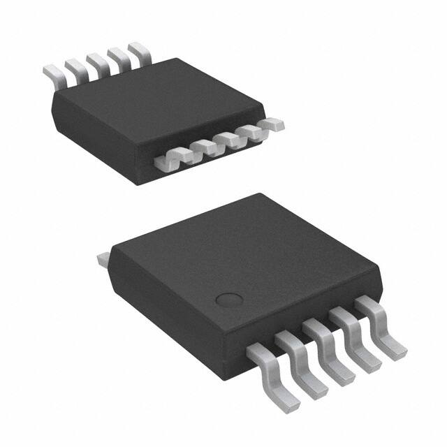
The DG2034E is available in MSOP10 and QFN12
3 mm x 3 mm packages.
APPLICATIONS
BENEFITS
• Power down fault protection
• Low parasitic and charge injection
• High ESD tolerance
• Automatic test equipment
• Process control and automation
• Data acquisition systems
• Meters and instruments
• Medical and healthcare systems
• Communication systems
• Audio and video switching
• Relay replacements
FUNCTIONAL BLOCK DIAGRAM AND PIN CONFIGURATION
12-Pin QFN (3 mm x 3 mm)
A0
NC
A1
12
11
10
MSOP-10
Logic
S1
1
9
S2
GND
2
8
COM
S3
3
7
S4
4
5
6
EN
NC
V+
10
A1
2
9
S2
GND
3
8
COM
S3
4
7
S4
EN
5
6
V+
A0
1
S1
Logic
Top View
Top View
S17-0388-Rev. A, 20-Mar-17
Document Number: 73172
1
For technical questions, contact: powerictechsupport@vishay.com
THIS DOCUMENT IS SUBJECT TO CHANGE WITHOUT NOTICE. THE PRODUCTS DESCRIBED HEREIN AND THIS DOCUMENT
ARE SUBJECT TO SPECIFIC DISCLAIMERS, SET FORTH AT www.vishay.com/doc?91000
�DG2034E
www.vishay.com
Vishay Siliconix
TRUTH TABLE
ORDERING INFORMATION
A1
A0
EN
ON SWITCH
X
X
0
None
0
0
1
S1
0
1
1
S2
1
0
1
S3
1
1
1
S4
TEMP. RANGE
-40 °C to +85 °C
PACKAGE
PART NUMBER
MSOP-10
DG2034EDQ-T1-GE3
12-pin QFN
(3 mm x 3 mm)
DG2034EDN-T1-GE4
ABSOLUTE MAXIMUM RATINGS
PARAMETER
LIMIT
Referenced V+ to GND
-0.3 to +6
AX, EN, SX, COM a
-0.3 to (V+ + 0.3)
Continuous current (any terminal)
± 50
Peak current (pulsed at 1 ms, 10 % duty cycle)
± 100
Power dissipation (package) b
QFN-12 (3 mm x 3 mm) c
1295
MSOP-10 d
320
Storage temperature (D suffix)
-65 to +150
ESD / HBM
EIA / JESD22-A114-A
8k
ESD / CDM
EIA / JESD22-C101-A
2k
JESD78
400
Latch up
UNIT
V
mA
mW
°C
V
mA
Notes
a. Signals on SX, COM, EN or AX exceeding V+ or V- will be clamped by internal diodes. Limit forward diode current to maximum current ratings
b. All leads welded or soldered to PC board
c. Derate 16.2 mV/°C above 70 °C
d. Derate 4 mV/°C above 70 °C
S17-0388-Rev. A, 20-Mar-17
Document Number: 73172
2
For technical questions, contact: powerictechsupport@vishay.com
THIS DOCUMENT IS SUBJECT TO CHANGE WITHOUT NOTICE. THE PRODUCTS DESCRIBED HEREIN AND THIS DOCUMENT
ARE SUBJECT TO SPECIFIC DISCLAIMERS, SET FORTH AT www.vishay.com/doc?91000
�DG2034E
www.vishay.com
Vishay Siliconix
SPECIFICATIONS (V+ = 3 V)
PARAMETER
SYMBOL
Analog Switch
Analog signal range d
TEST CONDITIONS
OTHERWISE UNLESS SPECIFIED
V+ = 3 V, ± 10 %, VAL = 0.5 V, VAH = 1.5 V e
VANALOG
V+ = 1.8 V, VS = 0.4 V / V+, IS = 8 mA
Drain-source
On-resistance
RDS(on)
V+ = 2.7 V, VCOM = 0.8 V / 1.8 V ICOM = 10 mA
RDS(on)
On-resistance matching
On-resistance flatness
d, f
Off leakage current g
COM off leakage current
Rflat(on)
IS(off)
g
Channel-on leakage current g
Digital Control
Input current d
Input high voltage d
Input low voltage d
Digital input capacitance d
Dynamic Characteristics
ICOM(off)
ICOM(on)
IA or IEN
VAH or VENH
VAL or VENL
CIN
Turn-on time
tON
Turn-off time
tOFF
Break-before-make time d
tBBM
Transition time
ttrans
Charge injection d
Bandwidth d
QINJ
BW
Off-isolation d
OIRR
Channel-to-channel crosstalk d
XTALK
V+ = 2.7 V, VCOM = 0.8 V / 1.4 V / 1.8 V
ICOM = 10 mA
V+ = 3.3 V, VS = 1 V / 3 V
VCOM = 3 V / 1 V, VEN = 0 V
V+ = 3.3 V
VCOM = VS = 1 V / 3 V
VA/EN = 0 V or V+, see truth table
VS = 1.5 V, CL = 35 pF, RL = 300
VS = 1.5 V / 0 V, VS = 0 V / 1.5 V, RL = 300
CL = 1 nF, Vgen = 1.5 V, Rgen = 0
CL = 5 pF (set up capacitance)
f = 1 MHz
RL = 50 , CL = 5 pF
f = 10 MHz
f = 1 MHz
RL = 50 , CL = 5 pF
f = 10 MHz
LIMITS
-40 to +85 °C
TEMP. a
MIN. c
UNIT
TYP. b MAX. c
Full
Room
Full
Room
Full
Room
Full
Room
Full
Room
Full
Room
Full
Room
Full
0
-2
-5
-2
-5
-2
-5
7
4.6
0.02
0.62
0.01
0.01
0.01
-
V+
10
11
5.3
5.9
0.27
0.41
1
1.3
2
5
2
5
2
5
Full
Full
Full
Room
-1
1.5
-
0.05
1.25
1
3
1
0.5
-
Room
Full
Room
Full
Room
Full
Room
Full
Room
Room
Room
Room
Room
Room
Room
Room
Room
7
5
-
19
16
12
26
-2
166
-67
-52
-71
-55
7
27
33
29
39
26
36
41
51
-
V
nA
μA
V
pF
ns
pC
MHz
dB
Off capacitance d
CS(off)
COM off capacitance d
CCOM(off)
V+ = 2.7 V, f = 1 MHz
pF
COM on capacitance d
CCOM(on)
Power Supply
Power supply range
V+
Full
2.7
3.3
V
Power supply current d
I+
V+ = 2.7 V, VA/EN = 0 V or 2.7 V, see truth table
Full
1
μA
Notes
a. Room = 25 °C, Full = as determined by the operating suffix
b. Typical values are for design aid only, not guaranteed nor subject to production testing
c. The algebraic convention whereby the most negative value is a minimum and the most positive a maximum, is used in this datasheet
d. Guarantee by design, not subjected to production test
e. VA, EN = input voltage to perform proper function
f. Difference of min. and max. values
g. Guaranteed by 5 V testing
S17-0388-Rev. A, 20-Mar-17
Document Number: 73172
3
For technical questions, contact: powerictechsupport@vishay.com
THIS DOCUMENT IS SUBJECT TO CHANGE WITHOUT NOTICE. THE PRODUCTS DESCRIBED HEREIN AND THIS DOCUMENT
ARE SUBJECT TO SPECIFIC DISCLAIMERS, SET FORTH AT www.vishay.com/doc?91000
�DG2034E
www.vishay.com
Vishay Siliconix
SPECIFICATIONS (V+ = 5 V)
PARAMETER
Analog Switch
Analog signal range d
Drain-source
On-resistance
On-resistance matching
On-resistance flatness d, f
Off leakage current g
SYMBOL
TEST CONDITIONS
OTHERWISE UNLESS SPECIFIED
V+ = 5 V, ± 10 %, VAL = 0.5 V, VAH = 2 V e
VANALOG
RDS(on)
RDS(on)
Rflat(on)
IS(off)
V+ = 4.5 V, VCOM = 0.8 V / 3.5 V
ICOM = 10 mA
V+ = 4.5 V, VCOM = 0.8 V / 2.5 V / 3.5 V
ICOM = 10 mA
V+ = 5.5 V, VS = 1 V / 4.5 V
VCOM = 4.5 V / 1 V, VEN = 0 V
COM off leakage current g
ICOM(off)
Channel-on leakage current g
ICOM(on)
V+ = 5.5 V, VCOM = VS = 1 V / 4.5 V
IPD
V+ = 0 V, VD = 5.5 V, SX open
V+ = 0 V, VS = 5.5 V, COM, open
Power down leakage d
Digital Control
Input current d
Input high voltage d
Input low voltage d
Digital input capacitance d
Dynamic Characteristics
IA or IEN
VAH or VENH
VAL or VENL
CIN
Turn-on time
tON
Turn-off time
tOFF
Break-before-make time d
tBBM
Transition time
ttrans
Propagation delay d
Charge injection d
Bandwidth d
tPD
QINJ
BW
Off-isolation d
OIRR
Channel-to-channel crosstalk d
XTALK
VA/EN = 0 V or V+, see truth table
VS = 3 V, CL = 35 pF, RL = 300
VS = 3 V / 0 V, VS = 0 V / 3 V, RL = 300
V+ = 5 V, no RLOAD
CL = 1 nF, Vgen = 2.5 V, Rgen = 0
CL = 5 pF (set up capacitance)
f = 1 MHz
RL = 50 , CL = 5 pF
f = 10 MHz
f = 1 MHz
RL = 50 , CL = 5 pF
f = 10 MHz
TEMP. a
LIMITS
-40 to +85 °C
UNIT
MIN. c TYP. b MAX. c
Full
Room
Full
Room
Full
Room
Full
Room
Full
Room
Full
Room
Full
Full
Full
0
-2
-8
-5
-15
-5
-15
-
2.5
0.02
0.6
0.17
0.77
0.61
0.01
0.01
V+
3.1
4
0.29
0.42
0.9
1.2
2
8
5
15
5
15
5
5
Full
Full
Full
Room
2
-
0.01
1.76
1.3
3
1
0.5
-
Room
Full
Room
Full
Room
Full
Room
Full
Room
Room
Room
Room
Room
Room
Room
Room
Room
Room
4
3
-
13
12
10
17
537
-2.6
166
-67
-52
-71
-55
7
27
36
25
35
20
30
32
42
-
V
nA
μA
μA
V
pF
ns
ps
pC
MHz
dB
CS(off)
Off capacitance d
COM off capacitance d
CCOM(off)
V+ = 5 V, f = 1 MHz
pF
CCOM(on)
COM on capacitance d
Power Supply
Power supply range
V+
Full
4.5
5.5
V
Power supply current d
I+
V+ = 5.5 V, VA/EN = 0 V or 5.5 V, see truth table
Full
1
μA
Notes
a. Room = 25 °C, Full = as determined by the operating suffix
b. Typical values are for design aid only, not guaranteed nor subject to production testing
c. The algebraic convention whereby the most negative value is a minimum and the most positive a maximum, is used in this datasheet
d. Guarantee by design, not subjected to production test
e. VA, EN = input voltage to perform proper function
f. Difference of min. and max. values
g. Guaranteed by 5 V testing
Stresses beyond those listed under “Absolute Maximum Ratings” may cause permanent damage to the device. These are stress ratings only, and functional operation
of the device at these or any other conditions beyond those indicated in the operational sections of the specifications is not implied. Exposure to absolute maximum
rating conditions for extended periods may affect device reliability.
S17-0388-Rev. A, 20-Mar-17
Document Number: 73172
4
For technical questions, contact: powerictechsupport@vishay.com
THIS DOCUMENT IS SUBJECT TO CHANGE WITHOUT NOTICE. THE PRODUCTS DESCRIBED HEREIN AND THIS DOCUMENT
ARE SUBJECT TO SPECIFIC DISCLAIMERS, SET FORTH AT www.vishay.com/doc?91000
�DG2034E
www.vishay.com
Vishay Siliconix
TYPICAL CHARACTERISTICS (25 °C, unless otherwise noted)
Axis Title
Axis Title
20
10000
1000
12
V+ = +2.7 V
10
8
V+ = +3 V
6
100
V+ = +4.5 V
4
-3000
ICOM(ON), VCOM = 1 V
-5000
ICOM(OFF), VCOM = 1 V,
VS = 4.5 V
-7000
IS(OFF), VCOM = 1 V, VS = 4.5 V
-9000
100
ICOM(ON), VCOM = 4.5 V
-11000
ICOM(OFF), VCOM = 4.5 V, VS = 1 V
-13000
V+ = +5 V
0
0
1
2
V+ = +5.5 V
10
3
4
-15000
5
10
-40
-20
0
80
Leakage Current vs. Temperature
Axis Title
+25 °C
1st line
2nd line
4
3
100
-40 °C
V+ = +2.7 V
IS = 10 mA
1.5
2
2.5
-400
1000
ICOM(OFF), VCOM = 1 V, VS = 3 V
IS(OFF), VCOM = 1 V, VS = 3 V
100
ICOM(ON), VCOM = 3 V
-600
ICOM(OFF), VCOM = 3 V, VS = 1 V
V+ = +3.3 V
10
1
ICOM(ON), VCOM = 1 V
-200
1st line
2nd line
1000
2nd line
Leakage Current (pA)
0
5
0.5
10000
IS(OFF), VCOM = 3 V, VS = 1 V
6
0
-800
3
10
-40
-20
0
20
40
60
80
VCOM - Analog Voltage (V)
2nd line
Temperature (°C)
2nd line
On-Resistance vs. Analog Voltage
Leakage Current vs. Temperature
10
9
+25 °C
1st line
2nd line
1000
2
100
-40 °C
V+ = +4.5 V
IS = 10 mA
10
1
1.5
8
V+ = +5.5 V
7
1000
6
5
4
100
3
V+ = +2.7 V
2
1
0
0.5
2nd line
I+ - Supply Current (nA)
+85 °C
10000
VA/EN = V+
1st line
2nd line
10000
1
100
Axis Title
Axis Title
4
3
100
200
+85 °C
0
60
On-Resistance vs. Analog Voltage
10000
1
40
Temperature (°C)
2nd line
Axis Title
2
20
VCOM - Analog Voltage (V)
2nd line
7
2nd line
RON - On-Resistance (Ω)
1000
1st line
2nd line
1000
2nd line
Leakage Current (pA)
14
2
2nd line
RON - On-Resistance (Ω)
10000
IS(OFF), VCOM = 4.5 V, VS = 1 V
-1000
16
1st line
2nd line
2nd line
RON - On-Resistance (Ω)
IS = 10 mA
V+ = +1.8 V
18
2
2.5
3
3.5
4
4.5
5
0
10
-40
-20
0
20
40
60
80
VCOM - Analog Voltage (V)
2nd line
Temperature (°C)
2nd line
On-Resistance vs. Analog Voltage
Supply Current vs. Temperature
S17-0388-Rev. A, 20-Mar-17
100
Document Number: 73172
5
For technical questions, contact: powerictechsupport@vishay.com
THIS DOCUMENT IS SUBJECT TO CHANGE WITHOUT NOTICE. THE PRODUCTS DESCRIBED HEREIN AND THIS DOCUMENT
ARE SUBJECT TO SPECIFIC DISCLAIMERS, SET FORTH AT www.vishay.com/doc?91000
�DG2034E
www.vishay.com
Vishay Siliconix
TYPICAL CHARACTERISTICS (25 °C, unless otherwise noted)
10000
1000
18
V+ = +3 V, tOFF
16
V+ = +5 V, tON
100
14
2nd line
Loss, OIRR, XTALK (dB)
V+ = +3 V, tON
20
1st line
2nd line
2nd line
tON(EN), tOFF(EN) - Switching Time (ns)
22
12
V+ = +5 V, tOFF
10
10
-50
-25
0
25
50
75
100
Axis Title
10
Loss
0
-10
-20
-30
-40
OIRR
-50
-60
XTALK
-70
-80
-90
-100
V+ = +5 V
-110
100K
1M
10M
100M
10000
1000
1st line
2nd line
Axis Title
24
100
10
1G
Temperature (°C)
2nd line
Frequency (Hz)
2nd line
Switching Time vs. Temperature
Loss, OIRR, XTALK vs. Frequency
Axis Title
Axis Title
1000
10000
100
V+ = +3 V
1000
12
10
8
100
6
V+ = +5 V
4
2nd line
I+ - Supply Current (μA)
16
1st line
2nd line
2nd line
tBBM - Switching Time (ns)
18
14
10000
10
V+ = +5 V
1000
1
1st line
2nd line
20
0.1
V+ = +2.7 V
0.01
100
0.001
0.0001
2
0.00001
0
10
10
-50
-25
0
25
50
75
100
100
1000
10K
100K
1M
10
10M
VA/EN Switching Frequency (Hz)
2nd line
Temperature (°C)
2nd line
Positive Supply Current vs. Switching Frequency
Switching Time vs. Temperature
Axis Title
35
V+ = +3 V
30
1000
25
20
15
100
V+ = +5 V
10
5
0
10
-50
-25
0
25
50
75
Temperature (°C)
2nd line
100
2nd line
VT - Switching Threshold (V)
10000
1st line
2nd line
2nd line
tTRANS - Switching Time (ns)
40
3.0
2.8
2.6
2.4
2.2
2.0
1.8
1.6
1.4
1.2
1.0
0.8
0.6
0.4
0.2
0
10000
-40 °C to +85 °C
1000
VIH = -40 °C
1st line
2nd line
Axis Title
100
VIL = 85 °C
10
1
2
3
4
5
6
V+ - Supply Voltage (V)
2nd line
Switching Threshold vs. Supply Voltage
Switching Time vs. Temperature
S17-0388-Rev. A, 20-Mar-17
Document Number: 73172
6
For technical questions, contact: powerictechsupport@vishay.com
THIS DOCUMENT IS SUBJECT TO CHANGE WITHOUT NOTICE. THE PRODUCTS DESCRIBED HEREIN AND THIS DOCUMENT
ARE SUBJECT TO SPECIFIC DISCLAIMERS, SET FORTH AT www.vishay.com/doc?91000
�DG2034E
www.vishay.com
Vishay Siliconix
TYPICAL CHARACTERISTICS (25 °C, unless otherwise noted)
Axis Title
Axis Title
10000
10000
10 000
1000
1000
-10
-20
100
V+ = 1.8 V
-30
V+ = 3 V
10
1
2
V+ = 5 V
1000
10
1
V+ = 2.7 V
100
0.1
0.01
-40
0
100
1st line
2nd line
V+ = 5 V
0
2nd line
I+ - Supply Current (μA)
10
1st line
2nd line
2nd line
QINJ - Charge Injection (pC)
20
3
4
5
0.001
6
10
0
0.5 1.0 1.5 2.0 2.5 3.0 3.5 4.0 4.5 5.0
VS - Analog Voltage (V)
2nd line
VA/EN (V)
2nd line
Charge Injection vs. Source Voltage
Positive Supply Current vs. Logic Voltage
4000
2000
IS(off)
Leakage Current (pA)
0
-2000
-4000
-6000
ICOM(on)
-8000
-10 000
ICOM(off)
-12 000
-14 000
V+ = +5.5 V
-16 000
0
1
2
3
4
VD - Analog Voltage (V)
5
6
Leakage Current vs. Analog Voltage
S17-0388-Rev. A, 20-Mar-17
Document Number: 73172
7
For technical questions, contact: powerictechsupport@vishay.com
THIS DOCUMENT IS SUBJECT TO CHANGE WITHOUT NOTICE. THE PRODUCTS DESCRIBED HEREIN AND THIS DOCUMENT
ARE SUBJECT TO SPECIFIC DISCLAIMERS, SET FORTH AT www.vishay.com/doc?91000
�DG2034E
www.vishay.com
Vishay Siliconix
TEST CIRCUITS
V+
Logic
Input
VINH
tr < 5 ns
tf < 5 ns
50 %
VINL
Switch
Input
VIN
Switch
Output
V+
NO or NC
COM
tOFF
VOUT
VOUT
IN
RL
300
GND
CL
35 pF
Note:
RL
VOUT = VIN
0V
Switch
Output
CL (includes fixture and stray capacitance)
0.9 x VOUT
90 %
tON
Logic input waveform is inverted for switches that
have the opposite logic sense control
RL + rON
Fig. 1 - Switching Time
V+
V+
VNO
VNC
tr < 5 ns
tf < 5 ns
VINL
COM
NO
VINH
Logic
Input
VO
NC
RL
300
IN
CL
35 pF
GND
VNC = VNO
VO
Switch
Output
90 %
0V
tD
tD
50 %
tr < 5 ns
tf < 5 ns
CL (includes fixture and stray capacitance)
Fig. 2 - Break-Before-Make
+15 V
V+
NO or NC
COM
VS1
VS2
VO
Logic VINH
Input
VINL
NC or NO
RL
300
IN
tTRANS+
CL
35 pF
tTRANS-
VS1
V01
GND
90 %
Switch
Output
CL (includes fixture and stray capacitance)
VO = VS
VS2
V02
10 %
RL
RL + rON
Fig. 3 - Transition Time
S17-0388-Rev. A, 20-Mar-17
Document Number: 73172
8
For technical questions, contact: powerictechsupport@vishay.com
THIS DOCUMENT IS SUBJECT TO CHANGE WITHOUT NOTICE. THE PRODUCTS DESCRIBED HEREIN AND THIS DOCUMENT
ARE SUBJECT TO SPECIFIC DISCLAIMERS, SET FORTH AT www.vishay.com/doc?91000
�DG2034E
www.vishay.com
Vishay Siliconix
TEST CIRCUITS
VO
V+
VO
V+
Rg
COM
NO or NC
IN
Vg
IN
VO
OFF
ON
CL
1 nF
OFF
Q = VO x CL
GND
IN dependent on switch configuration Input polarity determined
by sense of switch.
VIN = 0 - V+
Fig. 4 - Charge Injection
V+
C
V+
VS
VIN
NO or NC
COM
Rg = 50
50
IN
0 V or 2.4 V
NC or NO
VOUT
GND
VOUT
XTALK Isolation = 20 log
VIN
C = RF bypass
Fig. 5 - Crosstalk
V+
V+
C
C
V+
COM
NO or NC
COM
Meter
Rg = 50
IN
RL
50
IN
0 V, 2.4 V
0 V, 2.4 V
NO or NC
GND
GND
Off Isolation = 20 log
C = RF Bypass
Fig. 6 - Off Isolation
S17-0388-Rev. A, 20-Mar-17
VCOM
HP4192A
Impedance
Analyzer
or Equivalent
f = 1 MHz
VNO/NC
Fig. 7 - Source / Drain Capacitances
Document Number: 73172
9
For technical questions, contact: powerictechsupport@vishay.com
THIS DOCUMENT IS SUBJECT TO CHANGE WITHOUT NOTICE. THE PRODUCTS DESCRIBED HEREIN AND THIS DOCUMENT
ARE SUBJECT TO SPECIFIC DISCLAIMERS, SET FORTH AT www.vishay.com/doc?91000
�DG2034E
www.vishay.com
Vishay Siliconix
TEST CIRCUITS
V+
V+
NC, NO, Sx
COM
IN
GND
A
5.5 V
+
-
V+
V+
5.5 V
A
+
-
NC, NO, Sx
COM
IN
GND
Fig. 8 - Source / Drain Power Down Leakage
Vishay Siliconix maintains worldwide manufacturing capability. Products may be manufactured at one of several qualified locations. Reliability data for Silicon
Technology and Package Reliability represent a composite of all qualified locations. For related documents such as package / tape drawings, part marking, and
reliability data, see www.vishay.com/ppg?73172.
S17-0388-Rev. A, 20-Mar-17
Document Number: 73172
10
For technical questions, contact: powerictechsupport@vishay.com
THIS DOCUMENT IS SUBJECT TO CHANGE WITHOUT NOTICE. THE PRODUCTS DESCRIBED HEREIN AND THIS DOCUMENT
ARE SUBJECT TO SPECIFIC DISCLAIMERS, SET FORTH AT www.vishay.com/doc?91000
�Package Information
Vishay Siliconix
MSOP:
10−LEADS
JEDEC Part Number: MO-187, (Variation AA and BA)
(N/2) Tips)
2X
5
A B C 0.20
N N-1
0.60
0.48 Max
Detail “B”
(Scale: 30/1)
Dambar Protrusion
E
1 2
0.50
N/2
0.60
0.08 M C B S
b
A S
7
Top View
b1
e1
With Plating
e
A
See Detail “B”
c1
0.10 C
-H-
A1
D
6
Seating Plane
c
Section “C-C”
Scale: 100/1
(See Note 8)
Base Metal
-A-
3
See Detail “A”
Side View
0.25
BSC
C
Parting Line
0.07 R. Min
2 Places
C
ς
A2
Seating Plane
0.05 S
E1
-B-
L 4
T
-C-
3
0.95
End View
Detail “A”
(Scale: 30/1)
NOTES:
1.
2.
Dimensioning and tolerances per ANSI.Y14.5M-1994.
3.
Dimensions “D” and “E1” do not include mold flash or protrusions, and are
measured at Datum plane -H- , mold flash or protrusions shall not exceed
0.15 mm per side.
4.
Dimension is the length of terminal for soldering to a substrate.
5.
Terminal positions are shown for reference only.
6.
Formed leads shall be planar with respect to one another within 0.10 mm at
seating plane.
7.
N = 10L
Die thickness allowable is 0.203"0.0127.
The lead width dimension does not include Dambar protrusion. Allowable
Dambar protrusion shall be 0.08 mm total in excess of the lead width
dimension at maximum material condition. Dambar cannot be located on the
lower radius or the lead foot. Minimum space between protrusions and an
adjacent lead to be 0.14 mm. See detail “B” and Section “C-C”.
8.
Section “C-C” to be determined at 0.10 mm to 0.25 mm from the lead tip.
9.
Controlling dimension: millimeters.
10. This part is compliant with JEDEC registration MO-187, variation AA and BA.
11. Datums -A- and -B- to be determined Datum plane -H- .
12. Exposed pad area in bottom side is the same as teh leadframe pad size.
Document Number: 71245
12-Jul-02
MILLIMETERS
Dim
Min
Nom
Max
A
A1
A2
b
b1
c
c1
D
E
E1
e
e1
L
N
T
-
-
1.10
0.05
0.10
0.15
0.75
0.85
0.95
0.17
-
0.27
8
0.17
0.20
0.23
8
0.13
-
0.23
0.15
0.18
0.13
3.00 BSC
Note
3
4.90 BSC
2.90
3.00
3.10
3
0.70
4
0.50 BSC
2.00 BSC
0.40
0.55
10
0_
4_
5
6_
ECN: T-02080—Rev. C, 15-Jul-02
DWG: 5867
www.vishay.com
1
�Package Information
Vishay Siliconix
QFN−12 LEAD (3 X 3)
D2
D
D2/2
Terminal Tip
3
- B-
D/2
L
E2/2
E/2
e
E
E2
C
2xe
0.25
- A-
AA
DD
BB
Exposed Pad 4
4xb
0.10
CC
Pin #1 Identifier
M
C
A
B
0.25
3
C
2xe
TOP VIEW
BOTTOM VIEW
// 0.10
C
0.08
C
A
NX
4
A1
SEATING
PLANE - C A3
SIDE VIEW
MILLIMETERS
NOTES:
1.
All dimensions are in millimeters.
2.
N is the total number of terminals.
3.
Dimension b applies to metallized terminal and is measured
between 0.25 and 0.30 mm from terminal tip.
4.
Coplanarity applies to the exposed heat sink slug as well as the
terminal.
5.
The pin #1 identifier may be either a mold or marked feature, it
must be located within the zone iindicated.
INCHES
Dim
Min
Nom
Max
Min
Nom
Max
A
b
D
D2
E
E2
e
L
AA
BB
CC
DD
0.80
0.90
1.00
0.032
0.035
0.039
0.18
0.23
0.30
0.007
0.009
0.012
3.00 BSC
1.00
1.15
0.118 BSC
1.25
0.039
3.00 BSC
1.00
1.15
1.25
0.039
0.50 BSC
0.45
0.55
0.045
0.049
0.118 BSC
0.045
0.049
0.02 BSC
0.65
0.018
0.022
0.435
0.017
0.435
0.017
0.18
0.007
0.18
0.007
0.026
ECN: C-03092—Rev. A, 14-Apr-03
DWG: 5898
Document Number: 72209
14-Apr-03
www.vishay.com
1
�Legal Disclaimer Notice
www.vishay.com
Vishay
Disclaimer
ALL PRODUCT, PRODUCT SPECIFICATIONS AND DATA ARE SUBJECT TO CHANGE WITHOUT NOTICE TO IMPROVE
RELIABILITY, FUNCTION OR DESIGN OR OTHERWISE.
Vishay Intertechnology, Inc., its affiliates, agents, and employees, and all persons acting on its or their behalf (collectively,
“Vishay”), disclaim any and all liability for any errors, inaccuracies or incompleteness contained in any datasheet or in any other
disclosure relating to any product.
Vishay makes no warranty, representation or guarantee regarding the suitability of the products for any particular purpose or
the continuing production of any product. To the maximum extent permitted by applicable law, Vishay disclaims (i) any and all
liability arising out of the application or use of any product, (ii) any and all liability, including without limitation special,
consequential or incidental damages, and (iii) any and all implied warranties, including warranties of fitness for particular
purpose, non-infringement and merchantability.
Statements regarding the suitability of products for certain types of applications are based on Vishay’s knowledge of
typical requirements that are often placed on Vishay products in generic applications. Such statements are not binding
statements about the suitability of products for a particular application. It is the customer’s responsibility to validate that a
particular product with the properties described in the product specification is suitable for use in a particular application.
Parameters provided in datasheets and / or specifications may vary in different applications and performance may vary over
time. All operating parameters, including typical parameters, must be validated for each customer application by the customer’s
technical experts. Product specifications do not expand or otherwise modify Vishay’s terms and conditions of purchase,
including but not limited to the warranty expressed therein.
Except as expressly indicated in writing, Vishay products are not designed for use in medical, life-saving, or life-sustaining
applications or for any other application in which the failure of the Vishay product could result in personal injury or death.
Customers using or selling Vishay products not expressly indicated for use in such applications do so at their own risk.
Please contact authorized Vishay personnel to obtain written terms and conditions regarding products designed for
such applications.
No license, express or implied, by estoppel or otherwise, to any intellectual property rights is granted by this document
or by any conduct of Vishay. Product names and markings noted herein may be trademarks of their respective owners.
Revision: 13-Jun-16
1
Document Number: 91000
�