DG2599
Vishay Siliconix
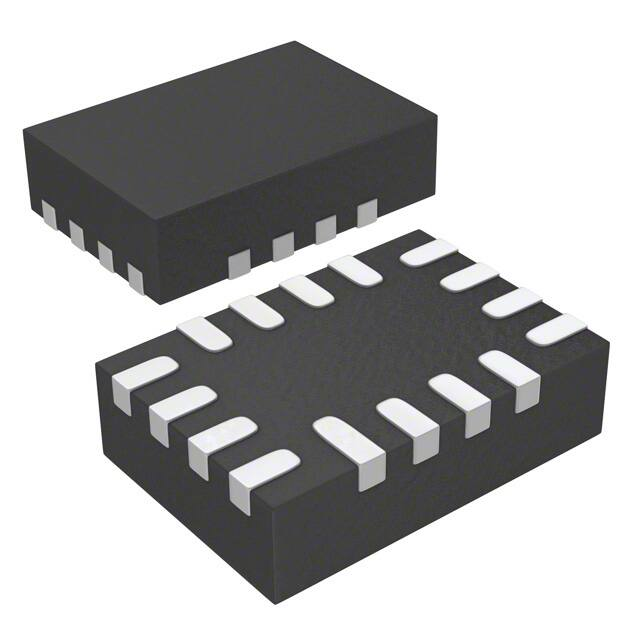
Low Voltage, Dual DPDT in miniQFN16
DESCRIPTION
FEATURES
The DG2599 is a CMOS Dual DPDT (Dual Double Pole
Double Throw) analog switch that operates over a wide
voltage range of 1.65 V to 5 V. It is optimized for portable
applications switching audio, SIM card signals, and other low
power signals.
The DG2599 features low ON resistance of 2.8 at 3 V
power supply, fast switching speed, and low power
consumption even when control logic signals are below V+
power supply voltage. The well matched dual DPDT switches
conduct signals equally in both directions. The DG2599 is
designed to guarantee break before make switching.
As a committed partner to the community and the
environment, Vishay Siliconix manufactures this product with
lead (Pb)-free device terminations. DG2599 are offered in a
miniQFN package. The miniQFN package has a nickel
palladium- gold device termination and is represented by the
lead (Pb)-free “-E4” suffix. The nickel-palladium-gold device
terminations meet all JEDEC standards for reflow and MSL
ratings.
• Halogen-free according to IEC 61249-2-21
definition
• Low voltage operation - 1.65 V to 5 V
•
•
•
•
Low on-resistance - 2.8 at V+ = 3 V
Power off protection on COM1 and COM2 pins
Latch up current great than 300 mA per JESD78
Compliant to RoHS Directive 2002/95/EC
APPLICATIONS
•
•
•
•
•
•
•
Cellular phones
PMPs and PDAs
Modems and peripherals
Computers and ebooks
Tablet devices
Displays and gaming
STB
ORDERING INFORMATION
Part Number
DG2599DN-T1-GE4
Package
miniQFN16 1.8 mm x 2.6 mm
COM1 NO1 V+ NC4
16
15
14
TRUTH TABLE (DG2599)
13
Logic
NC1
12 COM4
1
IN1, IN2
2
11 NO4
NO2
3
10 IN3, IN4
COM2
4
9
NC3
NC1, 2, 3 and 4
NO 1, 2, 3 and 4
0
ON
OFF
1
OFF
ON
Device Marking: A xx
xx = Date/Lot Traceability Code
(Top View)
5
6
7
8
Axx
NC2 GND NO3 COM3
Top View
Pin 1
Note: Pin 1 has long lead
Document Number: 67667
S11-1029-Rev. C, 23-May-11
www.vishay.com
1
This document is subject to change without notice.
THE PRODUCTS DESCRIBED HEREIN AND THIS DOCUMENT ARE SUBJECT TO SPECIFIC DISCLAIMERS, SET FORTH AT www.vishay.com/doc?91000
�DG2599
Vishay Siliconix
ABSOLUTE MAXIMUM RATINGS (TA = 25 °C, unless otherwise noted)
Parameter
Reference to GND
V+
Symbol
Limit
- 0.3 to 5
IN, COM, NC, NOa
- 0.3 to (V+ + 0.3)
Current (any terminal except NO, NC or COM)
Unit
V
30
Continuous Current (NO, NC, or COM)
± 300
Peak Current (pulsed at 1 ms, 10 % duty cycle)
± 500
Storage Temperature (D Suffix)
mA
- 65 to 150
Package Solder Reflow Conditionsd
miniQFN16
250
Power Dissipation (Packages)b
miniQFN16c
525
°C
mW
Notes:
a. Signals on NC, NO, or COM or IN exceeding V+ will be clamped by internal diodes. Limit forward diode current to maximum current ratings.
b. All leads welded or soldered to PC board.
c. Derate 6.6 mW/°C above 70 °C.
d. Manual soldering with iron is not recommended for leadless components. The miniQFN-16 is a leadless package. The end of the lead terminal
is exposed copper (not plated) as a result of the singulation process in manufacturing. A solder fillet at the exposed copper lip cannot be guaranteed and is not required to ensure adequate bottom side solder interconnection.
ELECTRICAL CHARACTERISTICS (V+ = 3 V)
Parameter
Test Conditions
Temp.
Min.
Full
1.65
VIN = 0 or V+
Full
Typ.
Max.
Unit
5
V
0.001
2
µA
V+
V
Power Supply and Signal
V+ Supply Voltage
V+ Supply Current
Analog Signal Range
Full
0
Switch On-Resistance and Leakage
Drain-Source On-Resistance
On-Resistance Flatness
Switch Off Leakage Current
Channel On-Leakage Current
V+ = 3 V, INO/NC = 100 mA, VCOM = 0.9 V, 2.3 V
V+ = 3 V, INO/NC = 100 mA, VCOM = 0 to V+
V+ = 4.3 V, VNO/NC = 0.3 V/4 V, VCOM = 4 V / 0.3 V
V+ = 4.3 V, VNO/NC and VCOM = 0.3 V / 4 V
Room
2.8
3.3
0.24
1.1
Full
3.6
Room
Full
1.3
Room
- 10
0.1
Full
- 100
Room
- 10
Full
- 100
10
100
0.1
10
nA
100
Digital Control
Input, High Voltage
Input, Low Voltage
Input, Bias Current
V+ = 4.3 V
Full
V+ = 3 V
V+ = 4.3 V
1.6
1.3
Full
0.6
V+ = 3 V
V
0.5
VIN = V+
Full
Turn On-Time
VCOM or VNO/NC = 3 V, RL = 50 , CL = 35 pF
Room
90
Full
115
Turn Off-Time
VCOM or VNO/NC = 3 V, RL = 50 , CL = 35 pF
Room
70
Full
85
Break Before Make Time
VCOM or VNO/NC = 3 V, RL = 50 , CL = 35 pF
Room
2
Full
2
CL = 1 nF, RGEN = 0
Room
-1
0.01
1
µA
Dynamic Characteristics
Charge Injection
± 10
Off Isolation
RL = 50 , CL = 5 pF, f = 1 MHz
- 66
Crosstalk
RL = 50 , CL = 5 pF, f = 1 MHz
Non-adjacent channels
- 110
CL = 5 pF, RL = 50
186
Source Off Capacitance
VIN = 0 or V+, f = 1 MHz
9
Channel On Capacitance
VIN = 0 or V+, f = 1 MHz
26
3dB Bandwith
www.vishay.com
2
ns
pC
dB
MHz
pF
Document Number: 67667
S11-1029-Rev. C, 23-May-11
This document is subject to change without notice.
THE PRODUCTS DESCRIBED HEREIN AND THIS DOCUMENT ARE SUBJECT TO SPECIFIC DISCLAIMERS, SET FORTH AT www.vishay.com/doc?91000
�DG2599
Vishay Siliconix
TYPICAL CHARACTERISTICS (TA = 25 °C, unless otherwise noted)
9
5.0
TA = 25 °C
INO/NC = 100 mA
8
4.0
RON - On-Resistance (Ω)
RON - On-Resistance (Ω)
V+ = 1.8 V
7
V+ = 2.5 V
6
V+ = 3 V
5
V+ = 3.6 V
V+ = 4 V
4
TA = 85 °C
4.5
V+ = 4.3 V
3
V+ = 5.5 V
2
TA = 25 °C
3.5
3.0
2.5
2.0
TA = - 40 °C
1.5
1.0
1
V+ = 2.5 V
INO/NC = 100 mA
0.5
0.0
0
0
1
2
3
4
VCOM - Analog Voltage (V)
5
0
6
0.5
1
1.5
2
RON vs. VCOM and Single Supply Voltage
RON vs. Analog Voltage and Temperature
3.0
4.0
TA = 85 °C
TA = 85 °C
TA = 25 °C
2.5
3.0
RON - On-Resistance (Ω)
RON - On-Resistance (Ω)
3.5
2.5
2.0
TA = - 40 °C
1.5
1.0
2.0
1.5
TA = 25 °C
1.0
TA = - 40 °C
0.5
V+ = 3 V
INO/NC = 100 mA
0.5
V+ = 4.3 V
INC/NO = 100 mA
0.0
0
0
0.5
1
1.5
2
2.5
3
0
0.5
RON vs. Analog Voltage and Temperature
1.5
2
2.5
3
3.5
4
RON vs. Analog Voltage and Temperature
10 000
100
V+ = 3 V
V+ = 3 V
1000
Leakage Current (pA)
10
1
0.1
100
ICOM(on)
- 40
- 20
0
20
40
60
Temperature (°C)
Supply Current vs. Temperature
Document Number: 67667
S11-1029-Rev. C, 23-May-11
80
100
ICOM(off)
10
INC(off)
1
0.01
0.001
- 60
1
VCOM - Analog Voltage (V)
VCOM - Analog Voltage (V)
I+ - Supply Current (nA)
2.5
VCOM - Analog Voltage (V)
- 40
- 20
0
20
40
60
80
100
Temperature (°C)
Leakage Current vs. Temperature
www.vishay.com
3
This document is subject to change without notice.
THE PRODUCTS DESCRIBED HEREIN AND THIS DOCUMENT ARE SUBJECT TO SPECIFIC DISCLAIMERS, SET FORTH AT www.vishay.com/doc?91000
�DG2599
Vishay Siliconix
TYPICAL CHARACTERISTICS (TA = 25 °C, unless otherwise noted)
50
100
V+ = 3 V
45
60
40
Leakage Current (pA)
ICOM(on)
ICOM(off)
40
tON, tOFF - Switching Time (ns)
80
20
0
INC(off)
- 20
- 40
- 60
tOFF V+ = 3 V
35
tON V+ = 3 V
30
25
tON V+ = 4.3 V
20
tOFF V+ = 4.3 V
15
10
- 80
5
- 100
0
0.5
1.0
1.5
2.0
2.5
0
- 60
3.0
- 40
- 20
Analog Voltage (V)
80
40
60
80
100
10
Loss
0
tON V+ = 3 V
70
- 10
- 20
60
Loss, OIRR, Xtalk (dB)
tON, tOFF - Switching Time (ns)
20
(NO) Switching Time vs. Temperature
Leakage vs. Analog Voltage
50
tON V+ = 4.3 V
40
30
20
- 30
OIRR
- 40
- 50
- 60
- 70
Xtalk NC/NO
- 80
- 90
Xtalk Ch3/C
- 100
tOFF V+ = 3 V
tOFF V+ = 4.3 V
10
0
- 60
0
Temperature (°C)
- 110
V+ = 3 V
RL = 50 Ω
- 120
- 40
- 20
0
20
40
60
80
- 130
100K
100
1M
10M
100M
1G
Frequency (Hz)
Temperature (°C)
Insertion Loss, Off Isolation and Crosstalk
(NC) Switching Time vs. Temperature
0.9
TA = 25 °C
VTH - Switching Threshold (V)
0.85
0.8
VINH
VINL
0.75
0.7
0.65
0.6
0.55
0.5
0.45
0.4
1
1.5
2
2.5
3
3.5
4
4.5
5
5.5
6
V+ - Supply Voltage (V)
Switching Threshold vs. Supply Voltage
www.vishay.com
4
Document Number: 67667
S11-1029-Rev. C, 23-May-11
This document is subject to change without notice.
THE PRODUCTS DESCRIBED HEREIN AND THIS DOCUMENT ARE SUBJECT TO SPECIFIC DISCLAIMERS, SET FORTH AT www.vishay.com/doc?91000
�DG2599
Vishay Siliconix
TEST CIRCUITS
V+
VINH
Logic
Input
50 %
V+
NO or NC
Switch
Input
VINL
Switch Output
COM
tr < 5 ns
tf < 5 ns
VOUT
0.9 x V OUT
Logic
Input
Switch
Output
IN
RL
50 Ω
GND
CL
35 pF
0V
tON
tOFF
0V
Logic “1” = Switch On
Logic input waveforms inverted for switches that have
the opposite logic sense.
CL (includes fixture and stray capacitance)
VOUT = VCOM
(R L
RL
+ R
ON
)
Figure 1. Switching Time
V+
Logic
Input
V+
VNO
VNC
COM
NO
VINH
tr < 5 ns
tf < 5 ns
VINL
VO
NC
RL
50 Ω
IN
CL
35 pF
GND
VNC = V NO
VO
90 %
Switch
0V
Output
tD
tD
CL (includes fixture and stray capacitance)
Figure 2. Break-Before-Make Interval
V+
Rgen
Δ VOUT
V+
NC or NO
COM
VOUT
VOUT
+
IN
IN
Vgen
CL = 1 nF
VIN = 0 - V+
On
Off
On
GND
Q = ΔVOUT x CL
IN depends on switch configuration: input polarity
determined by sense of switch.
Figure 3. Charge Injection
Document Number: 67667
S11-1029-Rev. C, 23-May-11
www.vishay.com
5
This document is subject to change without notice.
THE PRODUCTS DESCRIBED HEREIN AND THIS DOCUMENT ARE SUBJECT TO SPECIFIC DISCLAIMERS, SET FORTH AT www.vishay.com/doc?91000
�DG2599
Vishay Siliconix
TEST CIRCUITS
V+
V+
10 nF
10 nF
V+
V+
NC or NO
IN
COM
COM
0 V, 2.4 V
Meter
COM
IN
0 V, 2.4 V
RL
NC or NO
GND
HP4192A
Impedance
Analyzer
or Equivalent
GND
Analyzer
f = 1 MHz
VCOM
Off Isolation = 20 log V
NO / NC
Figure 4. Off-Isolation
Figure 5. Channel Off/On Capacitance
Vishay Siliconix maintains worldwide manufacturing capability. Products may be manufactured at one of several qualified locations. Reliability data for Silicon
Technology and Package Reliability represent a composite of all qualified locations. For related documents such as package/tape drawings, part marking, and
reliability data, see www.vishay.com/ppg?67667.
www.vishay.com
6
Document Number: 67667
S11-1029-Rev. C, 23-May-11
This document is subject to change without notice.
THE PRODUCTS DESCRIBED HEREIN AND THIS DOCUMENT ARE SUBJECT TO SPECIFIC DISCLAIMERS, SET FORTH AT www.vishay.com/doc?91000
�Package Information
www.vishay.com
Vishay Siliconix
Thin miniQFN16 Case Outline
B
12
0.10 C
Terminal tip (4)
16 x b
D
A
11
9
9
10
10
11
0.10 M C A B
0.05 M C
12
13
8
8
13
14
7
7
14
6
6
15
5
5
E
15
16
1
2
3
4
16
4
Pin #1 identifier (5)
15 x L
0.10 C
Top view
3
2
L1
1
e
Bottom view
0.10 C
C
A
Seating
plane
0.10 C
A3
Side view
DIMENSIONS
MILLIMETERS (1)
INCHES
MIN.
NOM.
MAX.
MIN.
NOM.
MAX.
A
0.50
0.55
0.60
0.020
0.022
0.024
A1
0
-
0.05
0
-
0.002
A3
0.15 ref.
b
0.15
D
2.50
e
0.006 ref.
0.20
0.25
0.006
2.60
2.70
0.098
0.40 BSC
E
1.70
1.80
0.008
0.010
0.102
0.106
0.016 BSC
1.90
0.067
0.071
0.075
L
0.35
0.40
0.45
0.014
0.016
0.018
L1
0.45
0.50
0.55
0.018
0.020
0.022
N (3)
16
16
Nd (3)
4
4
(3)
4
4
Ne
Notes
(1) Use millimeters as the primary measurement.
(2) Dimensioning and tolerances conform to ASME Y14.5M. - 1994.
(3) N is the number of terminals. Nd and Ne is the number of terminals in each D and E site respectively.
(4) Dimensions b applies to plated terminal and is measured between 0.15 mm and 0.30 mm from terminal tip.
(5) The pin 1 identifier must be existed on the top surface of the package by using identification mark or other feature of package body.
(6) Package warpage max. 0.05 mm.
ECN: T16-0226-Rev. B, 09-May-16
DWG: 6023
Revision: 09-May-16
Document Number: 64694
1
For technical questions, contact: analogswitchtechsupport@vishay.com
THIS DOCUMENT IS SUBJECT TO CHANGE WITHOUT NOTICE. THE PRODUCTS DESCRIBED HEREIN AND THIS DOCUMENT
ARE SUBJECT TO SPECIFIC DISCLAIMERS, SET FORTH AT www.vishay.com/doc?91000
�PAD Pattern
Vishay Siliconix
RECOMMENDED MINIMUM PADS FOR MINI QFN 16L
0.562
(0.0221)
0.400
(0.0157)
0.225
(0.0089)
1
2.900
(0.1142)
0.463
(0.0182)
1.200
(0.0472)
2.100
(0.0827)
Mounting Footprint
Dimensions in mm (inch)
Document Number: 66557
Revision: 05-Mar-10
www.vishay.com
1
�Legal Disclaimer Notice
www.vishay.com
Vishay
Disclaimer
ALL PRODUCT, PRODUCT SPECIFICATIONS AND DATA ARE SUBJECT TO CHANGE WITHOUT NOTICE TO IMPROVE
RELIABILITY, FUNCTION OR DESIGN OR OTHERWISE.
Vishay Intertechnology, Inc., its affiliates, agents, and employees, and all persons acting on its or their behalf (collectively,
“Vishay”), disclaim any and all liability for any errors, inaccuracies or incompleteness contained in any datasheet or in any other
disclosure relating to any product.
Vishay makes no warranty, representation or guarantee regarding the suitability of the products for any particular purpose or
the continuing production of any product. To the maximum extent permitted by applicable law, Vishay disclaims (i) any and all
liability arising out of the application or use of any product, (ii) any and all liability, including without limitation special,
consequential or incidental damages, and (iii) any and all implied warranties, including warranties of fitness for particular
purpose, non-infringement and merchantability.
Statements regarding the suitability of products for certain types of applications are based on Vishay’s knowledge of
typical requirements that are often placed on Vishay products in generic applications. Such statements are not binding
statements about the suitability of products for a particular application. It is the customer’s responsibility to validate that a
particular product with the properties described in the product specification is suitable for use in a particular application.
Parameters provided in datasheets and / or specifications may vary in different applications and performance may vary over
time. All operating parameters, including typical parameters, must be validated for each customer application by the customer’s
technical experts. Product specifications do not expand or otherwise modify Vishay’s terms and conditions of purchase,
including but not limited to the warranty expressed therein.
Except as expressly indicated in writing, Vishay products are not designed for use in medical, life-saving, or life-sustaining
applications or for any other application in which the failure of the Vishay product could result in personal injury or death.
Customers using or selling Vishay products not expressly indicated for use in such applications do so at their own risk.
Please contact authorized Vishay personnel to obtain written terms and conditions regarding products designed for
such applications.
No license, express or implied, by estoppel or otherwise, to any intellectual property rights is granted by this document
or by any conduct of Vishay. Product names and markings noted herein may be trademarks of their respective owners.
© 2017 VISHAY INTERTECHNOLOGY, INC. ALL RIGHTS RESERVED
Revision: 08-Feb-17
1
Document Number: 91000
�