DG2616, DG2617, DG2618
Vishay Siliconix
Low Voltage, Dual SPDT Analog Switch
with Charge Pump
DESCRIPTION
The DG2616, DG2617, DG2618 are monolithic CMOS
analog switching products designed for high performance
switching of analog signals. Combining low power, high
speed, low on-resistance and small physical size, the
DG2616, DG2617, DG2618 are ideal for portable and
battery powered applications.
The DG2616, DG2617, DG2618 have built-in charge-pump
circuitry which lowers the minimum supply voltage to + 1.5 V
while maintaining low on-resistance. The Control circuitry
allows the DG2616, DG2617, DG2618 to operate in different
configurations.
Built on Vishay Siliconix's low voltage process, the DG2616,
DG2617, DG2618 has an epitaxial layer that prevents
latch-up. Break-before-make is guaranteed.
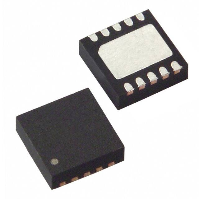
The DG2616, DG2617, DG2618 are manufactured in space
saving DFN-10 (3.0 x 3.0 mm). And as a committed partner
to the community and the environment, Vishay Siliconix
manufactures this product with lead (Pb)-free device
terminations and is 100 % RoHS compliant.
FEATURES
• Low voltage operation (1.5 V to 3.6 V)
• Low on-resistance - RON: 4.2 Ω typ. at 2.7 V
• Fast switching: tON = 39 ns
tOFF = 8 ns
• DFN-10 package
RoHS
COMPLIANT
BENEFITS
• Reduced power consumption
• High accuracy
• Reduce board space
• TTL/1.8 V logic compatible
• High bandwidth
APPLICATIONS
• Cellular phones
• Audio and video signal routing
• PCMCIA cards
• Battery operated systems
FUNCTIONAL BLOCK DIAGRAM AND PIN CONFIGURATION
TRUTH TABLE DG2616
TRUTH TABLE DG2618
Logic
NC1, 2
NO1, 2
0
ON
OFF
0
0
ON
1
OFF
ON
0
1
OFF
ON
ON
1
x
OFF
OFF
OFF
TRUTH TABLE DG2617
NO1, 2
Charge Pump
OFF
ON
ORDERING INFORMATION
SHDN/EN Logic
IN Logic
0
0
ON
OFF
ON
0
1
OFF
ON
ON
1
0
ON
OFF
OFF
1
1
OFF
ON
OFF
Document Number: 74411
S-82149-Rev. B, 08-Sep-08
SHDN/EN Logic IN Logic NC1, 2
NC1, 2 NO1, 2
Charge Pump
Temp. Range
- 40 °C to 85 °C
Package
Part Number
DFN-10
DG2616DN-T1-E4
DG2617DN-T1-E4
DG2618DN-T1-E4
www.vishay.com
1
�DG2616, DG2617, DG2618
Vishay Siliconix
DG2616
IN1
1
10
IN2
2
9
NC1
GND
3
8
NC2
COM1
4
7
NO1
COM2
5
6
NO2
V+
Top View
DG2617/DG2618
IN1
1
10
SHDN/EN
2
9
NC1
GND
3
8
NC2
COM1
4
7
NO1
COM2
5
6
NO2
V+
Top View
ABSOLUTE MAXIMUM RATINGS TA = 25 °C, unless otherwise noted
Parameter
Reference to GND
Current (Any terminal except NO, NC or COM)
Continuous Current (NO, NC, or COM)
Peak Current (Pulsed at 1 ms, 10 % Duty Cycle)
Storage Temperature (D-Suffix)
V+
IN, COM, NC, NOa
Limit
- 0.3 to 6.0
- 0.3 to (V+ + 0.3)
30
± 150
± 300
- 65 to 150
Unit
V
mA
°C
Package Solder Reflow Conditionsd
1191
mW
Power Dissipation (Packages)b
DFN-10c
Notes:
a. Signals on NC, NO, or COM or IN exceeding V+ will be clamped by internal diodes. Limit forward diode current to maximum current ratings.
b. All leads welded or soldered to PC board.
c. Derate 14.9 mW/°C above 70 °C
d. Manual soldering with iron is not recommended for leadless components. The DFN-10 is a leadless package. The end of the lead terminal is
exposed copper (not plated) as a result of the singulation process in manufacturing. A solder fillet at the exposed copper lip cannot be
guaranteed and is not required to ensure adequate bottom side solder interconnection.
www.vishay.com
2
Document Number: 74411
S-82149-Rev. B, 08-Sep-08
�DG2616, DG2617, DG2618
Vishay Siliconix
SPECIFICATIONS V+ = 3 V
Limits
- 40 °C to 85 °C
Test Conditions
Otherwise Unless Specified
Parameter
Symbol
V+ = 3 V, ± 10 %, VIN = 0.5 or 1.4 Ve
Temp.a
Min.b
Full
0
Typ.c
Max.b
Unit
V+
V
Analog Switch
Analog Signal Ranged
VNO, VNC,
VCOM
V+ = 1.5 V, VCOM = 1.5 V, INO, INC = 10 mA
V+ = 2.7 V, VCOM = 1.5 V, INO, INC = 10 mA
RON
On-Resistance
V+ = 2.7 V, VCOM = 2.7 V, INO, INC = 10 mA
Room
5.3
Full
4.2
Room
4.7
Full
V+ = 3.6 V, VCOM = 3.6 V, INO, INC = 10 mA
RON
RON Flatnessd
Flatness
V+ = 2.7 V, VCOM = 1.5 V, 2.7 V,
RON Matchd
ΔRON
INO, INC = 10 mA
On Resistance (Shutdown)
RSHDN
V+ = 3.6 V, VCOM = 1.7 V, INO, INC = 10 mA
INO(off),
Switch Off Leakage Current
INC(off)
ICOM(off)
Channel-On Leakage
Current
ICOM(on)
7.0
8.0
7.0
8.0
Room
5.5
Full
7.0
8.0
Room
0.6
Room
0.1
Room
15
Full
2.0
20
21
Room
-2
2
V+ = 3.6 V, VNO, VNC = 0.3 V/3.3 V,
Full
- 10
10
VCOM = 3.3 V/0.3 V
Room
-2
2
Full
- 10
10
V+ = 3.6 V, VNO, VNC = VCOM = 0.3 V/3.3 V
Ω
Room
-2
2
Full
- 10
10
nA
Digital Control
Input High Voltage
VINH
Input Low Voltage
VINL
Input Capacitance
Cin
IINL or IINH
Input Current
V+ = 1.5 V
1.0
V+ = 2.7 V to 3.6 V
1.4
V+ = 1.5 V
Full
0.4
V+ = 2.7 V to 3.6 V
0.5
Full
VIN = 0 or V+
V
Full
3.2
-1
pF
1
µA
Dynamic Characteristics
Room
tON
Turn-On Time
V+ = 2.7 or 3.6 V, VNO or VNC = 1.5 V,
tOFF
Turn-Off Time
Break-Before-Make Time
Charge Injection
d
RL = 50 Ω, CL = 35 pF
td
QINJ
OIRR
RL = 50 Ω, CL = 5 pF, f = 100 MHz
RL = 50 Ω, CL = 5 pF, f = 1 MHz
Crosstalkd, f
NO, NC Off Capacitanced
Channel-On Capacitanced
Document Number: 74411
S-82149-Rev. B, 08-Sep-08
XTALK
9
39
Full
Room
RL = 50 Ω, CL = 5 pF, f = 1 MHz
Off-Isolationd
69
76
Room
Full
CL = 1 nF, VGEN = 0 V, RGEN = 0 Ω
39
Full
1
7
Room
RL = 50 Ω, CL = 5 pF, f = 100 MHz
- 32
- 80
Room
9
Room
7
Room
21
Room
19
CNC(on)
dB
- 32
CNC(off)
f = 1 MHz
pC
- 77
CNO(off)
CNO(on)
ns
41
pF
www.vishay.com
3
�DG2616, DG2617, DG2618
Vishay Siliconix
SPECIFICATIONS V+ = 3 V
Limits
- 40 °C to 85 °C
Test Conditions
Otherwise Unless Specified
Parameter
Symbol
V+ = 3 V, ± 10 %, VIN = 0.5 or 1.4 Ve
Temp.a
Min.b
Typ.c
Max.b
Unit
3.6
V
104
300
0.1
2
Power Supply
Power Supply Range
Power Supply Current
V+
I+
1.5
V+ = 3.6 V, VIN = 0 or V+, SHDN/EN = 0 V
V+ = 3.6 V, VIN = 0 or V+, SHDN/EN = V+
Full
µA
Notes:
a. Room = 25 °C, Full = as determined by the operating suffix.
b. The algebraic convention whereby the most negative value is a minimum and the most positive a maximum, is used in this data sheet.
c. Typical values are for design aid only, not guaranteed nor subject to production testing.
d. Guarantee by design, not subjected to production test.
e. VIN = input voltage to perform proper function.
f. Crosstalk measured between channels.
Stresses beyond those listed under “Absolute Maximum Ratings” may cause permanent damage to the device. These are stress ratings only, and functional operation
of the device at these or any other conditions beyond those indicated in the operational sections of the specifications is not implied. Exposure to absolute maximum
rating conditions for extended periods may affect device reliability.
www.vishay.com
4
Document Number: 74411
S-82149-Rev. B, 08-Sep-08
�DG2616, DG2617, DG2618
Vishay Siliconix
TYPICAL CHARACTERISTICS TA = 25 °C, unless otherwise noted
13
10
V+ = 4.2 V
V+ = 5.0 V
12
9
V+ = 2.7 V, Is = 10 mA
+ 85 °C
+ 25 °C
- 40 °C
8
10
R ON - On-Resistance (Ω)
R ON - On-Resistance (Ω)
11
V+ = 1.5 V
9
V+ = 1.2 V
8
V+ = 2.7 V
V+ = 3.0 V
V+ = 3.6 V
V+ = 2.0 V
7
6
5
4
3
7
6
5
4
3
2
2
T = 25 °C
1
INO/NC = 10 mA
1
0
0
0
1
2
3
4
5
0.0
0.5
1.0
1.5
2.0
2.5
3.0
VCOM - Analog Voltage (V)
VCOM - Analog Voltage (V)
RON vs. VCOM and Supply Voltage
RON vs. Analog Voltage and Temperature
10
200
9
7
6
I+ - Supply Current (µA)
R ON - On-Resistance (Ω)
V+ = 3.6 V
V+ = 3.6 V, Is = 10 mA
+ 85 °C
+ 25 °C
- 40 °C
8
5
4
3
150
100
50
2
1
0
0.0
0.5
1.0
1.5
2.0
2.5
3.0
3.5
0
- 60
4.0
- 40
- 20
0
20
40
60
Temperature (°C)
RON vs. Analog Voltage and Temperature
Supply Current vs. Temperature
1000
100
500
400
V+ = 3.6V
V+ = 3.6 V
Leakage Current (pA)
300
Leakage Current (pA)
80
VCOM - Analog Voltage (V)
100
I COM(off)
INO(off)
I COM(on)
10
200
I COM(on)
100
INO(off) /INC(off)
0
- 100
ICOM(off)
- 200
- 300
- 400
1
- 60
- 40
- 20
0
20
40
60
80
Temperature (°C)
Leakage Current vs. Temperature
Document Number: 74411
S-82149-Rev. B, 08-Sep-08
100
- 500
0.0
0.6
1.2
1.8
2.4
3.0
3.6
VCOM - Analog Voltage (V)
Leakage vs. Analog Voltage
www.vishay.com
5
�DG2616, DG2617, DG2618
Vishay Siliconix
TYPICAL CHARACTERISTICS TA = 25 °C, unless otherwise noted
10
Loss
0
35
- 10
t ON V+ = 2.7 V
30
LOSS, OIRR, XTALK (dB)
tON, t OFF - Switching Time (ns)
40
t ON V+ = 3.6 V
25
20
15
10
t OFF V+ = 2.7 V
- 20
- 30
- 40
- 50
OIRR
- 60
XTalk
- 70
V+ = 2.7 V
- 80
5
t OFF V+ = 3.6 V
0
- 60
- 40
- 20
0
20
40
RL = 50 Ω
- 90
60
80
- 100
100k
100
1M
10M
100M
1G
Frequency (Hz)
Temperature (°C)
Switching Time vs. Temperature
Insertion Loss, Off-Isolation
Crosstalk vs. Frequency
30
2.0
Q - Charge Injection (pC)
V T - Switching Threshold (V)
25
1.5
1.0
0.5
V+ = 2.7 V
V+ = 2.0 V
20
15
V+ = 3.6 V
10
5
0
-5
0.0
1
www.vishay.com
6
2
3
4
5
6
- 10
0.0
0.5
1.0
1.5
2.0
2.5
3.0
3.5
V+ - Supply Voltage (V)
VCOM - Analog Voltage (V)
Switching Threshold vs. Supply Voltage
Charge Injection vs. Analog Voltage
4.0
Document Number: 74411
S-82149-Rev. B, 08-Sep-08
�DG2616, DG2617, DG2618
Vishay Siliconix
TEST CIRCUITS
V+
VINH
Logic
Input
V+
NO or NC
Switch
Input
VINL
Switch Output
COM
tr < 5 ns
tf < 5 ns
50 %
VOUT
0.9 x V OUT
Logic
Input
Switch
Output
IN
RL
50 Ω
GND
CL
35 pF
0V
tON
tOFF
0V
Logic "1" = Switch On
Logic input waveforms inverted for switches that have
the opposite logic sense.
CL (includes fixture and stray capacitance)
VOUT = VCOM
(R L
RL
+ R
ON
)
Figure 1. Switching Time
V+
Logic
Input
V+
COM
NO
VNO
VINH
tr < 5 ns
tf < 5 ns
VINL
VO
NC
VNC
RL
50 Ω
IN
CL
35 pF
GND
VNC = V NO
VO
90 %
Switch
0V
Output
tD
tD
CL (includes fixture and stray capacitance)
Figure 2. Break-Before-Make Interval
V+
Rgen
Δ VOUT
V+
COM
NC or NO
VOUT
VOUT
+
IN
IN
Vgen
CL = 1 nF
VIN = 0 - V+
On
Off
On
GND
Q = ΔVOUT x CL
IN depends on switch configuration: input polarity
determined by sense of switch.
Figure 3. Charge Injection
Document Number: 74411
S-82149-Rev. B, 08-Sep-08
www.vishay.com
7
�DG2616, DG2617, DG2618
Vishay Siliconix
TEST CIRCUITS
V+
V+
10 nF
10 nF
V+
V+
NC or NO
IN
COM
COM
0 V, 2.4 V
Meter
COM
IN
0 V, 2.4 V
RL
NC or NO
GND
HP4192A
Impedance
Analyzer
or Equivalent
GND
Analyzer
f = 1 MHz
VCOM
Off Isolation = 20 log V
NO / NC
Figure 4. Off-Isolation
Figure 5. Channel Off/On Capacitance
Vishay Siliconix maintains worldwide manufacturing capability. Products may be manufactured at one of several qualified locations. Reliability data for Silicon
Technology and Package Reliability represent a composite of all qualified locations. For related documents such as package/tape drawings, part marking, and
reliability data, see http://www.vishay.com/ppg?74411.
www.vishay.com
8
Document Number: 74411
S-82149-Rev. B, 08-Sep-08
�Package Information
Vishay Siliconix
DFN-10 LEAD (3 X 3)
D
e
Terminal Tip
3
D/2
3
NXb
0.10
M
C
A
B
5
0.15
C
E2
NXL
Exposed Pad
Index Area
D/2 E/2
D2
0.15
5
BOTTOM VIEW
// 0.10
E/2
ÉÉÉÉ
ÉÉÉÉ
ÉÉÉÉ
ÉÉÉÉ
2x
Index Area
D/2 E/2
C
E
2x
TOP VIEW
C
A
4
NX
0.08
SEATING
PLANE
C
A1
A3
SIDE VIEW
MILLIMETERS
NOTES:
1.
All dimensions are in millimeters and inches.
2.
N is the total number of terminals.
3.
4.
5.
Dimension b applies to metallized terminal and is measured
between 0.15 and 0.30 mm from terminal tip.
Coplanarity applies to the exposed heat sink slug as well as the
terminal.
The pin #1 identifier may be either a mold or marked feature, it
must be located within the zone iindicated.
INCHES
Dim
Min
Nom
Max
Min
Nom
Max
A
0.80
0.90
1.00
0.031
0.035
0.039
A1
0.00
0.02
0.05
0.000
0.001
0.002
A3
b
D
D2
E
E2
e
L
0.20 BSC
0.18
0.23
0.008 BSC
0.30
0.007
2.48
0.087
3.00 BSC
2.20
2.38
1.64
0.40
0.094
0.098
0.118 BSC
1.74
0.059
0.50 BSC
0.30
0.012
0.118 BSC
3.00 BSC
1.49
0.009
0.065
0.069
0.020 BSC
0.50
0.012
0.016
0.020
*Use millimeters as the primary measurement.
ECN: S-42134—Rev. A, 29-Nov-04
DWG: 5943
Document Number: 73181
29-Nov-04
www.vishay.com
1
�Legal Disclaimer Notice
www.vishay.com
Vishay
Disclaimer
ALL PRODUCT, PRODUCT SPECIFICATIONS AND DATA ARE SUBJECT TO CHANGE WITHOUT NOTICE TO IMPROVE
RELIABILITY, FUNCTION OR DESIGN OR OTHERWISE.
Vishay Intertechnology, Inc., its affiliates, agents, and employees, and all persons acting on its or their behalf (collectively,
“Vishay”), disclaim any and all liability for any errors, inaccuracies or incompleteness contained in any datasheet or in any other
disclosure relating to any product.
Vishay makes no warranty, representation or guarantee regarding the suitability of the products for any particular purpose or
the continuing production of any product. To the maximum extent permitted by applicable law, Vishay disclaims (i) any and all
liability arising out of the application or use of any product, (ii) any and all liability, including without limitation special,
consequential or incidental damages, and (iii) any and all implied warranties, including warranties of fitness for particular
purpose, non-infringement and merchantability.
Statements regarding the suitability of products for certain types of applications are based on Vishay’s knowledge of typical
requirements that are often placed on Vishay products in generic applications. Such statements are not binding statements
about the suitability of products for a particular application. It is the customer’s responsibility to validate that a particular
product with the properties described in the product specification is suitable for use in a particular application. Parameters
provided in datasheets and/or specifications may vary in different applications and performance may vary over time. All
operating parameters, including typical parameters, must be validated for each customer application by the customer’s
technical experts. Product specifications do not expand or otherwise modify Vishay’s terms and conditions of purchase,
including but not limited to the warranty expressed therein.
Except as expressly indicated in writing, Vishay products are not designed for use in medical, life-saving, or life-sustaining
applications or for any other application in which the failure of the Vishay product could result in personal injury or death.
Customers using or selling Vishay products not expressly indicated for use in such applications do so at their own risk. Please
contact authorized Vishay personnel to obtain written terms and conditions regarding products designed for such applications.
No license, express or implied, by estoppel or otherwise, to any intellectual property rights is granted by this document or by
any conduct of Vishay. Product names and markings noted herein may be trademarks of their respective owners.
Material Category Policy
Vishay Intertechnology, Inc. hereby certifies that all its products that are identified as RoHS-Compliant fulfill the
definitions and restrictions defined under Directive 2011/65/EU of The European Parliament and of the Council
of June 8, 2011 on the restriction of the use of certain hazardous substances in electrical and electronic equipment
(EEE) - recast, unless otherwise specified as non-compliant.
Please note that some Vishay documentation may still make reference to RoHS Directive 2002/95/EC. We confirm that
all the products identified as being compliant to Directive 2002/95/EC conform to Directive 2011/65/EU.
Vishay Intertechnology, Inc. hereby certifies that all its products that are identified as Halogen-Free follow Halogen-Free
requirements as per JEDEC JS709A standards. Please note that some Vishay documentation may still make reference
to the IEC 61249-2-21 definition. We confirm that all the products identified as being compliant to IEC 61249-2-21
conform to JEDEC JS709A standards.
Revision: 02-Oct-12
1
Document Number: 91000
�


 工商网监
湘ICP备2023018690号
工商网监
湘ICP备2023018690号
