DG2717
Vishay Siliconix
Low-Voltage, 0.45-Ω, SPDT Analog Switch
DESCRIPTION
FEATURES
The DG2717 is a low voltage, low on resistance, single- pole/
double-throw (SPDT) monolithic CMOS analog switch
designed for high performance switching of analog signals.
Combining low-power, high speed, low on-resistance, and
small package size, the DG2717 is ideal for portable and
battery power applications.
•
•
•
•
•
•
The DG2717 has an operation range from 1.6 V to 4.3 V
single supply, and is low voltage logic compatible within this
range, allowing the easy interface with low voltage DSP or
MCU control logic. These traits make it ideal for one cell
Li-ion battery direct power.
The switch conducts signals within power rails equally well in
both directions when on, and blocks up to the power supply
level when off. Break-before-make is guaranteed.
The DG2717 is built on Vishay Siliconix’s sub micron CMOS
low voltage process.
As a committed partner to the community and the
environment, Vishay Siliconix manufactures this product
with lead (Pb)-free device terminations. For analog switching
products manufactured in SC89 package, the lead (Pb)-free
"E3" suffix is being used as a designator. It has a Tin device
termination that meets all JEDEC standards for reflow and
MSL rating.
Low Voltage Operation (1.6 V to 4.3 V)
Low On-Resistance - rDS(on): 0.45 Ω Typ.
Fast Switching - tON: 22 ns, tOFF: 8 ns
Low Leakage
TTL/CMOS Compatible
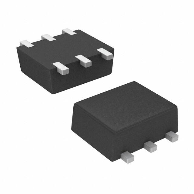
SC-89 (1.6 mm x 1.6 mm) Package
RoHS
COMPLIANT
BENEFITS
•
•
•
•
Reduced Power Consumption
Simple Logic Interface
High Accuracy
Reduce Board Space
APPLICATIONS
•
•
•
•
•
Cellular Phones
PMP/MP3
Audio and Video Signal Routing
Power Switch
Reed Relay Replacement
FUNCTIONAL BLOCK DIAGRAM AND PIN CONFIGURATION
TRUTH TABLE
SC-89
IN
1
6
NO (Source1)
V+
2
5
COM
GND
3
4
NC (Source2)
Logic
NC
NO
0
ON
OFF
1
OFF
ON
Top View
ORDERING INFORMATION
Pin 1
Bx
Temp Range
Package
Part Number
- 40 to 85 °C
SC89-6
DG2717DX-T1-E3
Device Marking: Bx
x = Date/Lot Traceability Code
Document Number: 73538
S-70852-Rev. B, 30-Apr-07
www.vishay.com
1
�DG2717
Vishay Siliconix
ABSOLUTE MAXIMUM RATINGS
Parameter
Limit
Reference V+ to GND
IN, COM, NC, NOa
V
- 0.3 to (V+ + 0.3)
Continuous Current (NO, NC and COM Pins)
± 200
Peak Current (Pulsed at 1 ms, 10 % duty cycle)
± 300
Storage Temperature (D Suffix)
Power Dissipation (Packages)
Unit
- 0.3 to + 5.0
- 65 to 150
°C
172
mW
6-Pin SC89
b
mA
Notes:
a. Signals on NC, NO, or COM or IN exceeding V+ will be clamped by internal diodes. Limit forward diode current to maximum current ratings.
b. All leads welded or soldered to PC Board.
c. Derate 2.15 mW/°C above 70 °C.
SPECIFICATIONS (V+ = 1.8 V)
Limits
- 40 to 85 °C
Test Condition
Otherwise Unless Specified
Parameter
Symbol
V+ = 1.8 V, ± 10 %, VIN = 0.4 or 1.0 Ve
Tempa
Minb
Full
0
Typc
Maxb
Unit
V+
V
2.0
2.1
Ω
Analog Switch
Analog Signal Ranged
On-Resistance
VNO, VNC,
VCOM
rON
V+ = 1.8 V, VCOM = 0.2 V, INO/NC = 100 mA
Room
Full
1.0
Digital Control
Input High Voltage
VINH
Full
Input Low Voltage
VINL
Full
Input Capacitanced
Cin
Full
f
Input Current
IINL or IINH
VIN = 0 V or V+
Full
1.0
0.4
7
-1
V
pF
1
µA
Dynamic Characteristics
Turn-On Timed
tON
Turn-Off Timed
tOFF
Break-Before-Make Timed
Charge Injectiond
d
QINJ
Off-Isolation
Crosstalkd
XTALK
Room
CL = 1 nF, VGEN = 0 V, RGEN = 0 Ω, Figure 3
Room
NO, NC Off Capacitanced
CNO(off),
CNC(off)
Channel-On Capacitanced
CON
VIN = 0 or V+, f = 1 MHz
74
81
14
34
35
Fulld
Room
RL = 50 Ω, CL = 5 pF, f = 1 MHz
54
Fulld
VNO or VNC = 1.5 V, RL = 50 Ω, CL = 35 pF
Figures 1 and 2
td
OIRR
www.vishay.com
2
Room
ns
8
26
Room
- 54
Room
- 60
Room
80
Room
180
pC
dB
pF
Document Number: 73538
S-70852-Rev. B, 30-Apr-07
�DG2717
Vishay Siliconix
SPECIFICATIONS (V+ = 3.0 V)
Limits
- 40 to 85 °C
Test Condition
Otherwise Unless Specified
Parameter
Symbol
V+ = 2.7 V to 3.6 V, VIN = 0.5 or 1.4 Ve
Tempa
Minb
Full
0
Typc
Maxb
Unit
V+
V
Analog Switch
Analog Signal Ranged
VNO, VNC,
VCOM
V+ = 2.7 V, VCOM = 1.5 V
INO, INC = 100 mA
Room
Full
0.5
0.7
0.8
V+ = 3.6 V, VCOM = 0.5 V, 2.0 V
INO, INC = 100 mA
Room
Full
0.45
0.65
0.75
rON
Flatness
V+ = 2.7 V, VCOM = 0.6 V, 2.1 V
INO, INC = 100 mA
Room
ΔrON
V+ = 2.7 V, VCOM = 1.5 V, INO, INC = 100 mA
rON
On-Resistance
rON Flatnessd
rON Matchd
Switch Off Leakage Current
INO(off),
INC(off)
ICOM(off)
Channel-On Leakage Current
ICOM(on)
V+ = 4.3 V
VNO, VNC = 0.3 V / 4 V, VCOM = 4 V / 0.3 V
V+ = 4.3 V, VNO, VNC = VCOM = 0.3 V / 4 V
Ω
0.2
Room
0.6
Room
Full
- 10
- 100
10
100
Room
Full
- 10
- 100
10
100
Room
Full
- 10
- 100
10
100
1.4
nA
Digital Control
Input High Voltage
VINH
Full
Input Low Voltage
VINL
Full
Input Capacitanced
Cin
Full
f
IINL or IINH
Input Current
VIN = 0 V or V+
Full
0.5
7
-1
V
pF
1
µA
Dynamic Characteristics
Turn-On Time
tON
Turn-Off Time
tOFF
Break-Before-Make Time
Charge Injection
Off-Isolation
d
d
Crosstalkd
Channel-On
td
QINJ
OIRR
XTALK
NO, NC Off Capacitanced
Capacitanced
V+ = 3.0 V, VNO or VNC = 1.5 V
RL = 300 Ω, CL = 35 pF
Figure 1 and 2
CNO(off),
CNC(off)
Room
Full
22
44
48
Room
Full
8
29
30
Room
CL = 1 nF, VGEN = 0 V, RGEN = 0 Ω, Figure 3
RL = 50 Ω, CL = 5 pF, f = 1 MHz
VIN = 0 or V+, f = 1 MHz
CON
ns
1
Room
28
Room
- 54
Room
- 57
Room
76
Room
178
pC
dB
pF
Power Supply
Power Supply Range
V+
Power Supply Current
I+
1.6
V+ = 3.6 V, VIN = 0 or V+
0.01
4.3
V
1.0
µA
Notes:
a. Room = 25 °C, Full = as determined by the operating suffix.
b. The algebraic convention whereby the most negative value is a minimum and the most positive a maximum, is used in this data sheet.
c. Typical values are for design aid only, not guaranteed nor subject to production testing.
d. Guarantee by design, nor subjected to production test.
e. VIN = input voltage to perform proper function.
Stresses beyond those listed under “Absolute Maximum Ratings” may cause permanent damage to the device. These are stress ratings only, and functional operation
of the device at these or any other conditions beyond those indicated in the operational sections of the specifications is not implied. Exposure to absolute maximum
rating conditions for extended periods may affect device reliability.
Document Number: 73538
S-70852-Rev. B, 30-Apr-07
www.vishay.com
3
�DG2717
Vishay Siliconix
TYPICAL CHARACTERISTICS 25 °C, unless otherwise noted
1.0
2.00
V+ = 1.6 V
1.75
V+ = 3.6 V
IS = 100 mA
T = 25 °C
IS = 100 mA
r ON - On-Resistance (Ω)
r ON - On-Resistance (Ω)
0.8
1.50
1.25
V+ = 1.8 V
1.00
V+ = 2.3 V
V+ = 2.7 V
V+ = 3.0 V
0.75
0.50
V+ = 3.6 V
0.25
85 °C
25 °C
0.4
0.2
- 40 °C
V+ = 3.2 V
V+ = 4.3 V
0.00
0.0
0.6
0.5
1.0
1.5
2.0
2.5
3.0
3.5
0.0
0.0
4.0
0.6
1.2
1.8
2.4
3.0
3.6
VCOM - Analog Voltage (V)
VCOM - Analog Voltage (V)
rON vs. Analog Voltage and Temperature
rON vs. VCOM and Single Supply Voltage
100 m
10000
1000
1m
I+ - Supply Current (A)
I+ - Supply Current (nA)
10 m
V+ = 4.3 V
V+ = 3.6 V
100
10
V+ = 4.3 V
100 µ
10 µ
V+ = 3.6 V
1µ
100 n
10 n
1
- 40
1n
- 15
10
35
60
85
100
1K
Temperature (°C)
10 K
100 K
1M
10 M
Input Switching Frequency (Hz)
Supply Current vs. Temperature
Supply Current vs. Input Switching Frequency
1000
10000
V+ = 3.6 V
800
V+ = 3.6 V
600
Leakage Current (pA)
Leakage Current (pA)
1000
INC(off)
100
ICOM(off)
10
400
200
INC(off)
ICOM(off)
ICOM(on)
0
- 200
- 400
- 600
ICOM(on)
- 800
1
- 40
- 15
10
35
60
Temperature (°C)
Leakage Current vs. Temperature
www.vishay.com
4
85
- 1000
0.0
0.6
1.2
1.8
2.4
3.0
3.6
VCOM, VNO, VNC - Analog Voltage
Leakage vs. Analog Voltage
Document Number: 73538
S-70852-Rev. B, 30-Apr-07
�DG2717
Vishay Siliconix
TYPICAL CHARACTERISTICS 25 °C, unless otherwise noted
t ON, t OFF - Switching Time (ns)
60.00
tON V+ = 1.6 V
50.00
40.00
tON V+ = 1.8 V
tON V+ = 2.3 V
30.00
tON V+ = 3.3 V
20.00
tOFF V+ = 1.6 V
tON V+ = 3.0 V
tON V+ = 4.3 V
tOFF V+ = 1.8 V
10.00
0.00
- 40
tOFF V+ = 4.3 V
- 15
10
tOFF V+ = 2.3 V
tOFF V+ = 3.0 V
tOFF V+ = 3.3 V
35
60
85
Temperature (°C)
2.00
300
1.75
250
V+ = 4.3 V
Q - Charge Injection (pC)
V T - Switching Threshold (V)
Switching Time vs. Temperature
1.50
1.25
1.00
0.75
0.50
200
150
V+ = 3 V
100
50
V+ = 1.8 V
0
0.25
0.00
1.0
1.5
2.0
2.5
3.0
3.5
4.0
4.5
5.0
- 50
0.0
0.6
1.2
1.8
2.4
3.0
3.6
V+ - Supply Voltage (V)
VCOM - Analog Voltage (v)
Switching Threshold vs. Supply Voltage
Charge Injection vs. Analog Voltage
4.2
10
0
Loss, OIRR, XTALK (dB)
LOSS
- 10
- 20
- 30
- 40
OIRR
- 50
- 60
V+ = 3.0 V
RL = 50 Ω
XTALK
- 70
- 80
10 K
100K
1M
10 M
100 M
1G
Frequency (Hz)
Insertion Loss, Off-Isolation, Crosstalk vs. Frequency
Document Number: 73538
S-70852-Rev. B, 30-Apr-07
www.vishay.com
5
�DG2717
Vishay Siliconix
TEST CIRCUITS
V+
Logic
Input
VINH
VINL
V+
Switch Output
COM
NO or NC
Switch
Input
tr < 5 ns
tf < 5 ns
50 %
VOUT
0.9 x VOUT
Switch
Output
IN
Logic
Input
RL
50 Ω
GND
CL
35 pF
0V
tOFF
tON
Logic “1” = Switch On
Logic input waveforms inverted for switches that have
the opposite logic sense.
CL (includes fixture and stray capacitance)
V COM
V OUT
RL
RL
R ON
Figure 1. Switching Time
V+
Logic
Input
V+
VNO
VNC
tr < 5 ns
tf < 5 ns
VINL
COM
NO
VINH
VO
NC
RL
50 Ω
IN
CL
35 pF
GND
VNC = VNO
VO
Switch
Output
90 %
0V
tD
tD
CL (includes fixture and stray capacitance)
Figure 2. Break-Before-Make Interval
V+
Rgen
ΔVOUT
V+
COM
NC or NO
VOUT
VOUT
+
Vgen
IN
CL = 1 nF
IN
On
On
Off
GND
Q = ΔVOUT x CL
VIN = 0 - V+
IN depends on switch configuration: input polarity
determined by sense of switch.
Figure 3. Charge Injection
www.vishay.com
6
Document Number: 73538
S-70852-Rev. B, 30-Apr-07
�DG2717
Vishay Siliconix
TEST CIRCUITS
V+
10 nF
V+
NC or NO
IN
0 V, 2.4 V
COM
Off Isolation
RL
GND
V COM
20 log V
NO NC
Analyzer
Figure 4. Off-Isolation
V+
10 nF
V+
COM
Meter
IN
0 V, 2.4 V
NC or NO
GND
HP4192A
Impedance
Analyzer
or Equivalent
f = 1 MHz
Figure 5. Channel Off/On Capacitance
Vishay Siliconix maintains worldwide manufacturing capability. Products may be manufactured at one of several qualified locations. Reliability data for Silicon Technology and Package Reliability represent a composite of all qualified locations. For related documents such as package/tape drawings, part marking, and reliability
data, see http://www.vishay.com/ppg?73538.
Document Number: 73538
S-70852-Rev. B, 30-Apr-07
www.vishay.com
7
�Legal Disclaimer Notice
Vishay
Disclaimer
All product specifications and data are subject to change without notice.
Vishay Intertechnology, Inc., its affiliates, agents, and employees, and all persons acting on its or their behalf
(collectively, “Vishay”), disclaim any and all liability for any errors, inaccuracies or incompleteness contained herein
or in any other disclosure relating to any product.
Vishay disclaims any and all liability arising out of the use or application of any product described herein or of any
information provided herein to the maximum extent permitted by law. The product specifications do not expand or
otherwise modify Vishay’s terms and conditions of purchase, including but not limited to the warranty expressed
therein, which apply to these products.
No license, express or implied, by estoppel or otherwise, to any intellectual property rights is granted by this
document or by any conduct of Vishay.
The products shown herein are not designed for use in medical, life-saving, or life-sustaining applications unless
otherwise expressly indicated. Customers using or selling Vishay products not expressly indicated for use in such
applications do so entirely at their own risk and agree to fully indemnify Vishay for any damages arising or resulting
from such use or sale. Please contact authorized Vishay personnel to obtain written terms and conditions regarding
products designed for such applications.
Product names and markings noted herein may be trademarks of their respective owners.
Document Number: 91000
Revision: 18-Jul-08
www.vishay.com
1
�