DG2718
New Product
Vishay Siliconix
0.45-W CMOS, 1.65-V to 3.6-V, Dual DPDT Analog Switch
FEATURES
BENEFITS
APPLICATIONS
D Low Voltage Operation (1.65 V to 3.6 V)
D Low On-Resistance - rON: 0.45 W @ 2.7 V
D Fast Switching: tON = 28 ns
tOFF = 17 ns
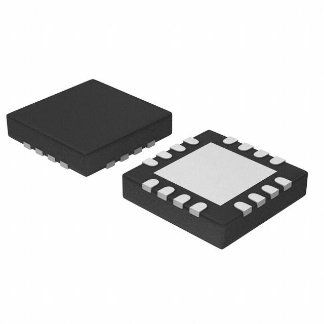
D QFN-16 (3x3) Package
D
D
D
D
D
D
D
D
D
D
Reduced Power Consumption
High Accuracy
Reduce Board Space
TTL/1.8-V Logic Compatible
High Bandwidth
Cellular Phones
Speaker Headset Switching
Audio and Video Signal Routing
PCMCIA Cards
Battery Operated Systems
DESCRIPTION
The DG2718 is a dual double-pole/double-throw monolithic
CMOS analog switch designed for high performance switching
of analog signals. Combining low power, high speed, low
on-resistance and small physical size, the DG2718 is ideal for
portable and battery powered applications requiring high
performance and efficient use of board space.
The DG2718 is built on Vishay Siliconix’s low voltage process. An
epitaxial layer prevents latchup. Break-before-make is
guaranteed.
The switch conducts equally well in both directions when on,
and blocks up to the power supply level when off.
FUNCTIONAL BLOCK DIAGRAM AND PIN CONFIGURATION
DG2718
QFN-16 (3 X 3)
COM1 NO1
16
15
V+
NC4
14
13
TRUTH TABLE
Logic
NC1
1
12
COM4
IN1, IN2
2
11
NO4
NO2
3
10
IN3, IN4
4
9
NC3
NC1, 2, 3 and 4
NO1, 2, 3 and 4
0
ON
OFF
1
OFF
ON
ORDERING INFORMATION*
COM2
Temp Range
Package
Part Number
-40 to 85°C
16-Pin QFN (3 x 3 mm)
Variation 2
DG2718DN–T1–E4
* Lead-Free Version Available
5
6
NC2
GND
7
8
NO3 COM3
Top View
NOTE:
Underside exposed pad has no device electrical connection. It
is recommended that no electrical connection is made to it.
Document Number: 72677
S–52186—Rev. B, 17-Oct-05
www.vishay.com
1
�DG2718
New Product
Vishay Siliconix
ABSOLUTE MAXIMUM RATINGS
Reference to GND
V+ . . . . . . . . . . . . . . . . . . . . . . . . . . . . . . . . . . . . . . . . . . . . . . . . . . -0.3 to +4.0 V
IN, COM, NC, NOa . . . . . . . . . . . . . . . . . . . . . . . . . . . . . . . -0.3 to (V+ + 0.3 V)
Current (Any terminal except NO, NC or COM) . . . . . . . . . . . . . . . . . . 30 mA
Continuous Current (NO, NC, or COM) . . . . . . . . . . . . . . . . . . . . . "300 mA
Peak Current . . . . . . . . . . . . . . . . . . . . . . . . . . . . . . . . . . . . . . . . . . . . "500 mA
(Pulsed at 1 ms, 10% duty cycle)
Storage Temperature (D Suffix) . . . . . . . . . . . . . . . . . . . . . . . . . . -65 to 150°C
Package Solder Reflow Conditionsd
16-Pin QFN (3 x 3 mm) . . . . . . . . . . . . . . . . . . . . . . . . . . . . . . . . . . . . . . 250°C
Power Dissipation (Packages)b
QFN-16c . . . . . . . . . . . . . . . . . . . . . . . . . . . . . . . . . . . . . . . . . . . . . . . 1385 mW
Notes:
a. Signals on NC, NO, or COM or IN exceeding V+ will be clamped by
internal diodes. Limit forward diode current to maximum current ratings.
b. All leads welded or soldered to PC Board.
c. Derate 17.3 mW/_C above 70_C
d. Manual soldering with iron is not recommended for leadless components.
The QFN is a leadless package. The end of the lead terminal is exposed
copper (not plated) as a result of the singulation process in
manufacturing. A solder fillet at the exposed copper lip cannot be
guaranteed and is not required to ensure adequate bottom side solder
interconnection.
Stresses beyond those listed under “Absolute Maximum Ratings” may cause permanent damage to the device. These are stress ratings only, and functional operation
of the device at these or any other conditions beyond those indicated in the operational sections of the specifications is not implied. Exposure to absolute maximum rating
conditions for extended periods may affect device reliability.
SPECIFICATIONS (V+ = 1.8 V)
Limits
Test Conditions
Otherwise Unless Specified
Parameter
Symbol
V+ = 1.8 V, VIN = 0.4 or 1.1 Ve
–40 to 85_C
Tempa
Minb
Full
0
Typc
Maxb
Unit
V+
V
2.0
2.8
W
Analog Switch
Analog Signal Ranged
On-Resistanced
VNO, VNC,
VCOM
rON
V+ = 1.8 V, VCOM = 0.2 V/0.9 V, INO, INC = 100 mA
Room
Full
0.7
Digital Control
Input High Voltage
VINH
Full
Input Low Voltage
VINL
Full
Input Capacitance
Input Current
0.4
Full
Cin
IINL or IINH
1.1
VIN = 0 or V+
Full
6
–1
V
pF
1
mA
Dynamic Characteristics
Room
Full
62
94
92
VNO or VNC = 1.5 V, RL = 50 W, CL = 35 pF
Room
Full
24
52
55
CL = 1 nF, VGEN = 0 V, RGEN = 0 W
Room
65
Room
–74
Room
–74
CNO(off)
Room
108
CNC(off)
Room
108
Room
225
Room
225
Turn-On Time
tON
Turn-Off Time
tOFF
Break-Before-Make Time
td
Charge Injectiond
QINJ
Off-Isolationd
OIRR
Crosstalkd
XTALK
NO, NC Off Capacitanced
Channel On
Channel-On
Capacitanced
CNO(on)
Full
RL = 50 W
W, CL = 5 pF
pF, f = 100 kHz
VIN = 0 or V+,
V+ f = 1 MHz
CNC(on)
ns
16
pC
dB
pF
Power Supply
Power Supply Current
www.vishay.com
2
I+
VIN = 0 or V+
Full
1.0
mA
Document Number: 72677
S–52186—Rev. B, 17-Oct-05
�DG2718
New Product
Vishay Siliconix
SPECIFICATIONS (V+ = 3 V)
Limits
Test Conditions
Otherwise Unless Specified
Parameter
Symbol
V+ = 3 V, "10%, VIN = 0.5 or 1.4 Ve
–40 to 85_C
Tempa
Minb
Full
0
Typc
Maxb
Unit
V+
V
Analog Switch
Analog Signal Ranged
On-Resistanced
rON Flatnessd
rON Matchd
Switch Off Leakage Current
VNO, VNC,
VCOM
rON
rON
Flatness
DrON
INO(off),
INC(off)
ICOM(off)
Channel-On Leakage Current
ICOM(on)
V+ = 2.7 V, VCOM = 0.2 V/1.5 V, INO, INC = 100 mA
V+ = 2.7 V
VCOM = 0 to V+
V+, INO, INC = 100 mA
V+ = 3.3 V, VNO, VNC = 0.3 V/3 V
VCOM = 3 V/0.3 V
V+ = 3.3 V, VNO, VNC = VCOM = 0.3 V/3 V
Room
Full
0.45
0.6
0.7
Room
0.1
0.15
Room
0.05
Room
Full
–1
–10
1
10
Room
Full
–1
–10
1
10
Room
Full
–1
–10
1
10
1.4
W
nA
Digital Control
Input High Voltage
VINH
Full
Input Low Voltage
VINL
Full
Input Capacitance
Input Current
Full
Cin
IINL or IINH
0.5
VIN = 0 or V+
Full
6
–1
V
pF
1
mA
Dynamic Characteristics
Room
Full
28
57
60
VNO or VNC = 1.5 V, RL = 50 W, CL = 35 pF
Room
Full
17
45
47
CL = 1 nF, VGEN = 0 V, RGEN = 0 W
Room
232
Room
–75
Room
–75
CNO(off)
Room
102
CNC(off)
Room
102
Room
234
Room
234
Turn-On Time
tON
Turn-Off Time
tOFF
Break-Before-Make Time
td
Charge Injectiond
QINJ
Off-Isolationd
OIRR
Crosstalkd
XTALK
NO, NC Off Capacitanced
Channel On Capacitanced
Channel-On
CNO(on)
Full
RL = 50 W
W, CL = 5 pF
pF, f = 100 kHz
VIN = 0 or V+,
V+ f = 1 MHz
CNC(on)
ns
1
pC
dB
pF
Power Supply
Power Supply Range
V+
Power Supply Current
I+
2.7
VIN = 0 or V+
Full
3.3
V
1.0
mA
Notes:
a.
b.
c.
d.
e.
f.
Room = 25°C, Full = as determined by the operating suffix.
The algebraic convention whereby the most negative value is a minimum and the most positive a maximum, is used in this data sheet.
Typical values are for design aid only, not guaranteed nor subject to production testing.
Guarantee by design, nor subjected to production test.
VIN = input voltage to perform proper function.
Guaranteed by 5-V leakage testing, not production tested.
Document Number: 72677
S–52186—Rev. B, 17-Oct-05
www.vishay.com
3
�DG2718
New Product
Vishay Siliconix
TYPICAL CHARACTERISTICS (25_C UNLESS NOTED)
rON vs. VCOM and Supply Voltage
rON vs. Analog Voltage and Temperature
1.50
0.8
T = 25_C
IS = 100 mA
V+ = 1.65 V
V+ = 1.8 V
1.00
V+ = 2.0 V
V+ = 2.3 V
0.75
V+ = 2.7 V
V+ = 3.0 V
0.50
IS = 100 mA
V+ = 3 V
0.7
r ON – On-Resistance ( W )
r ON – On-Resistance ( W )
1.25
85_C
0.6
25_C
–40_C
0.5
0.4
0.3
0.2
0.25
V+ = 3.3 V
0.00
0.0
0.5
1.0
1.5
2.0
2.5
0.1
V+ = 3.6 V
3.0
3.5
0.0
0.0
4.0
0.5
1.0
VCOM – Analog Voltage (V)
Supply Current vs. Temperature
2.0
2.5
3.0
Supply Current vs. Input Switching Frequency
10000
100 mA
10 mA
V+ = 3 V
VIN = 0 V
I+ – Supply Current (A)
1000
I+ – Supply Current (nA)
1.5
VCOM – Analog Voltage (V)
100
V+ = 2.7 V
1 mA
100 mA
10 mA
1 mA
100 nA
10
10 nA
1 nA
1
100 pA
–60
–40
–20
0
20
40
60
80
10
100
100
Temperature (_C)
10 K
100 K
1M
10 M
Input Switching Frequency (Hz)
Leakage Current vs. Temperature
Leakage vs. Analog Voltage
1000
300
250
V+ = 3.3 V
200
INO(off), INC(off)
Leakage Current (pA)
Leakage Current (pA)
1K
100
ICOM(off)
ICOM(on)
10
V+ = 3.3 V
ICOM(off)
150
INO(off), IINC(off)
100
50
0
–50
ICOM(on)
–100
–150
–200
–250
1
–60
–40
–20
0
20
40
Temperature (_C)
www.vishay.com
4
60
80
100
–300
0.00
0.50
1.00
1.50
2.00
2.50
3.00
VCOM, VNO, VNC – Analog Voltage (V)
Document Number: 72677
S–52186—Rev. B, 17-Oct-05
�DG2718
New Product
Vishay Siliconix
TYPICAL CHARACTERISTICS (25_C UNLESS NOTED)
Insertion Loss, Off-Isolation
Crosstalk vs. Frequency
Switching Time vs. Temperature
70
10
LOSS
60
–10
50
Loss, OIRR, X TALK (dB)
t ON / t OFF – Switching Time (m s)
tON V+ = 1.8 V
tON V+ = 2.3 V
40
tON V+ = 3.0 V
30
tOFF V+ = 1.8 V
tOFF V+ = 2.3 V
20
tOFF V+ = 3.0 V
XTALK
–30
OIRR
–50
V+ = 3 V
RL = 50 W
–70
10
0
–60
–90
–40
–20
0
20
40
60
80
100
100 K
1M
10 M
Temperature (_C)
1G
Charge Injection vs. Analog Voltage
2.00
250
1.75
200
1.50
Q – Charge Injection (pC)
– Switching Threshold (V)
Switching Threshold vs. Supply Voltage
VT
100 M
Frequency (Hz)
1.25
1.00
0.75
0.50
150
V+ = 3 V
100
V+ = 1.8 V
50
0
–50
0.25
0.00
1.0
1.5
2.0
2.5
3.0
3.5
–100
0.0
4.0
0.5
V+ – Supply Voltage (V)
1.0
1.5
2.0
2.5
3.0
VCOM – Analog Voltage (V)
TEST CIRCUITS
V+
Logic
Input
V+
Switch
Input
NO or NC
tr t 5 ns
tf t 5 ns
VOUT
0.9 x VOUT
IN
Logic
Input
50%
VINL
Switch Output
COM
VINH
RL
300 W
GND
CL
35 pF
Switch
Output
0V
tON
tOFF
0V
Logic “1” = Switch On
Logic input waveforms inverted for switches that have
the opposite logic sense.
CL (includes fixture and stray capacitance)
VOUT + VCOM
ǒ
RL
Ǔ
R L ) R ON
Figure 1.
Document Number: 72677
S–52186—Rev. B, 17-Oct-05
Switching Time
www.vishay.com
5
�DG2718
New Product
Vishay Siliconix
TEST CIRCUITS
V+
Logic
Input
V+
COM
NO
VNO
VINH
tr


 工商网监
湘ICP备2023018690号
工商网监
湘ICP备2023018690号
