DG2735, DG2736
Vishay Siliconix
Low Voltage, 0.6 , Dual SPDT Analog Switch
DESCRIPTION
FEATURES
The DG2735, DG2736 are low voltage, low on-resistance,
dual single-pole/double-throw (SPDT) monolithic CMOS
analog switches designed for high performance switching of
analog signals. Combining low-power, high speed, low
on-resistance, and small package size, the DG2735,
DG2736 are ideal for portable and battery power
applications.
The DG2735, DG2736 have an operation range from 1.65 V
to 4.3 V single supply. The DG2735 has two separate control
pins with for the separated two SPDT switched. The DG2736
has an EN pin. All switches are at high impedance mode
when the EN is high.
The DG2735, DG2736 are guaranteed 1.65 V logic
compatible, allowing the easy interface with low voltage DSP
or MCU control logic and ideal for one cell Li-ion battery
direct power.
The switch conducts signals within power rails equally well in
both directions when on, and blocks up to the power supply
level when off. Break-before-make is guaranteed.
The DG2735, DG2736 are built on Vishay Siliconix’s sub
micron CMOS low voltage process technology and provides
greater than 300 mA latch-up protection, as tested per
JESD78.
As a committed partner to the community and the
environment, Vishay Siliconix manufactures this product with
lead (Pb)-free device terminations. DG2735, DG2736 are
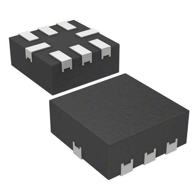
offered in a miniQFN package. The miniQFN package has a
nickel-palladium-gold device termination and is represented
by the lead (Pb)-free “-E4” suffix. The nickel-palladium-gold
device terminations meet all JEDEC standards for reflow and
MSL ratings.
•
•
•
•
•
•
Low voltage operation (1.65 V to 4.3 V)
Low on-resistance - RON: 0.6 at 2.7 V
Fast switching: tON = 55 ns at 2.7 V
TOFF = 40 ns at 2.7 V
Latch-up current > 300 mA (JESD78)
Material categorization: For definitions of compliance
please see www.vishay.com/doc?99912
BENEFITS
•
•
•
•
Reduced power consumption
High accuracy
Reduce board space
TTL/1.65 V logic compatible
APPLICATIONS
•
•
•
•
•
•
Cellular phones
Speaker headset switching
Audio and video signal routing
PCMCIA cards
Battery operated systems
Portable media player Handheld test instruments
FUNCTIONAL BLOCK DIAGRAM AND PIN CONFIGURATION
DG2735
miniQFN-10L
NC2
GND
NC2
GND
DG2736
miniQFN-10L
7
6
7
6
COM2
9
4
IN1
NO2
10
3
COM1
Pin 1: LONG LEAD
1
2
EN
8
5
NC1
COM2
9
4
IN1
NO2
10
3
COM1
Pin 1: LONG LEAD
1
2
NO1
NC1
V+
5
NO1
8
V+
IN2
Device Marking: Ax for DG2735
Device Marking: Bx for DG2736
x = Date/Lot Traceability Code
(Top View)
Ax
Pin 1
(Top View)
Bx
or
Pin 1
Note: Pin 1 has long lead
Document Number: 74420
S12-2498-Rev. D, 22-Oct-12
For technical questions, contact: analogswitchtechsupport@vishay.com
www.vishay.com
1
This document is subject to change without notice.
THE PRODUCTS DESCRIBED HEREIN AND THIS DOCUMENT ARE SUBJECT TO SPECIFIC DISCLAIMERS, SET FORTH AT www.vishay.com/doc?91000
�DG2735, DG2736
Vishay Siliconix
TRUTH TABLE
ORDERING INFORMATION
Logic
EN (DG2736 only)
NC1, 2
NO1, 2
0
1
OFF
OFF
1
1
OFF
OFF
0
0
ON
OFF
1
0
OFF
ON
Temp. Range
Package
- 40 °C to 85°C
Part Number
DG2735DN-T1-E4
DG2736DN-T1-E4
miniQFN10
ABSOLUTE MAXIMUM RATINGS (TA = 25 °C, unless otherwise noted)
Parameter
Symbol
V+
Reference to GND
IN, COM, NC, NOa
Current (Any terminal except NO, NC or COM)
Continuous Current (NO, NC, or COM)
Peak Current (Pulsed at 1 ms, 10 % duty cycle)
Storage Temperature (D Suffix)
Power Dissipation (Packages)b
miniQFN10c
Limit
- 0.3 to 5
- 0.3 to (V+ + 0.3)
30
± 250
± 500
- 65 to 150
208
Unit
V
mA
°C
mW
Notes:
a. Signals on NC, NO, or COM or IN exceeding V+ will be clamped by internal diodes. Limit forward diode current to maximum current ratings.
b. All leads welded or soldered to PC board.
c. Derate 4 mW/C above 70 °C.
SPECIFICATIONS (V+ = 3 V)
Parameter
Symbol
Limits
- 40 °C to 85 °C
Test Conditions
Unless Otherwise Specified
V+ = 3 V, ± 10 %,VIN = 0.4 V or 1.65 Ve
Temp.a
Min.b
RDS(on)
Full
0
Typ.c
Max.b
Unit
V+
V
Analog Switch
Analog Signal Ranged
Vanalog
V+ = 2.7 V, INO/NC = 100 mA, VCOM = 0.5 V
V+ = 2.7 V, INO/NC = 100 mA, VCOM = 1.5 V
V+ = 2.7 V, INO/NC = 100 mA, VCOM = 0.5 V
On-Resistance
RDS(on)
V+ = 2.7 V, INO/NC = 100 mA, VCOM = 1.5 V
V+ = 4.3 V, INO/NC = 100 mA, VCOM = 0.9 V
V+ = 4.3 V, INO/NC = 100 mA, VCOM = 2.5 V
V+ = 4.3 V, INO/NC = 100 mA, VCOM = 0.9 V
V+ = 4.3 V, INO/NC = 100 mA, VCOM = 2.5 V
RON Match
d
RON resistance flatnessd
Switch Off Leakage
Current
RON
RON
flatness
INO/NC(off)
ICOM(off)
Channel-On Leakage
Current
Document Number: 74420
S12-2498-Rev. D, 22-Oct-12
ICOM(on)
V+ = 2.7 V, INO/NC = 100 mA,
VCOM = 0.5 V, 1.5 V
V+ = 4.3 V, INO/NC = 100 mA,
VCOM = 0.9 V, 2.5 V
V+ = 2.7 V, INO/NC = 100 mA,
VCOM = 0.5 V, 1.5 V
V+ = 4.3 V, VNO/NC = 0.3 V/4 V,
VCOM = 4 V/0.3 V
V+ = 4.3 V, VNO/NC = VCOM = 4 V/0.3 V
Room
0.5
Full
0.5
0.4
Room
0.3
Full
0.5
Room
0.06
Room
0.6
0.5
0.08
0.15
Room
-2
2
10
Full
- 10
Room
-2
2
Full
- 10
10
Room
Full
-5
5
- 20
20
For technical questions, contact: analogswitchtechsupport@vishay.com
nA
www.vishay.com
2
This document is subject to change without notice.
THE PRODUCTS DESCRIBED HEREIN AND THIS DOCUMENT ARE SUBJECT TO SPECIFIC DISCLAIMERS, SET FORTH AT www.vishay.com/doc?91000
�DG2735, DG2736
Vishay Siliconix
SPECIFICATIONS (V+ = 3 V)
Parameter
Symbol
Test Conditions
Unless Otherwise Specified
V+ = 3 V, ± 10 %,VIN = 0.4 V or 1.65 Ve
Limits
- 40 °C to 85 °C
Temp.a
Min.b
1.65
Typ.c
Max.b
Unit
Digital Control
Input High Voltage
VINH
Full
Input Low Voltage
VINL
Full
Input Capacitance
Full
CIN
IINL or IINH
Input Current
VIN = 0 or V+
V
0.4
6
Full
-1
Room
1
pF
1
µA
Dynamic Characteristics
Break-Before-Make Timee
tBBM
Turn-On Timee
tON
Turn-Off Timee
tOFF
Enable Turn-On Timee
DG2736 (EN)
Enable Turn-Off Time
DG2736 (EN)
Room
Full
V+ = 3.6 V, VNO, VNC = 1.5 V, RL = 50 ,
CL = 35 pF
tON(EN)
OIRR
Crosstalkd
XTALK
3dB bandwithd
NO, NC Off Capacitanced
Channel On Capacitanced
Room
CNC(off)
58
50
78
60
Room
35
Full
RL = 50 , CL = 5 pF, f = 100 kHz
Room
RL = 50 , CL = 5 pF
Room
ns
80
58
60
- 70
dB
- 70
50
CNO(off)
CNO(on)
35
Full
Room
tOFF(EN)
78
80
Full
e
Off-Isolationd
5
50
MHz
55
VIN = 0 V, or V+, f = 1 MHz
55
Room
pF
130
130
CNC(on)
Power Supply
Power Supply Range
V+
Power Supply Current
I+
1.65
VIN = 0 or V+
Full
4.3
V
1
µA
Notes:
a. Room = 25 °C, Full = as determined by the operating suffix.
b. The algebraic convention whereby the most negative value is a minimum and the most positive a maximum, is used in this data sheet.
c. Typical values are for design aid only, not guaranteed nor subject to production testing.
d. Guarantee by design, not subjected to production test.
e. VIN = input voltage to perform proper function.
Stresses beyond those listed under “Absolute Maximum Ratings” may cause permanent damage to the device. These are stress ratings only, and functional operation
of the device at these or any other conditions beyond those indicated in the operational sections of the specifications is not implied. Exposure to absolute maximum
rating conditions for extended periods may affect device reliability.
Document Number: 74420
S12-2498-Rev. D, 22-Oct-12
For technical questions, contact: analogswitchtechsupport@vishay.com
www.vishay.com
3
This document is subject to change without notice.
THE PRODUCTS DESCRIBED HEREIN AND THIS DOCUMENT ARE SUBJECT TO SPECIFIC DISCLAIMERS, SET FORTH AT www.vishay.com/doc?91000
�DG2735, DG2736
Vishay Siliconix
TYPICAL CHARACTERISTICS (TA = 25 °C, unless otherwise noted)
0.6
2.4
V+ = 1.5 V
2.2
0.5
1.8
RON - On-Resistance (Ω)
R ON - On-Resistance (Ω)
+ 85 °C
TA = 25 °C
INO/NC = 100 mA
2.0
1.6
1.4
V+ = 1.8 V
1.2
1.0
0.8
V+ = 2.7 V
V+ = 3.0 V V+ = 3.6 V
0.6
0.4
+ 25 °C
0.3
- 40 °C
0.2
0.2
V+ = 4.3 V
0.0
0.0
0.0
0.5
1.0
1.5
2.0
2.5
3.0 3.5
4.0 4.5
0.0
5.0
1.0
1.5
2.0
2.5
3.0
VCOM - Analog Voltage (V)
VCOM - Analog Voltage (V)
RON vs. Analog Voltage and Temperature
1.0
+ 85 °C
0.9
0.5
0.8
R ON - On-Resistance (Ω)
+ 25 °C
0.4
0.3
- 40 °C
0.2
0.7
0.6
0.5
+ 85 °C
0.4
0.3
+ 25 °C
0.2
V+ = 2.7 V,
IS = 100 mA NC
0.1
V+ = 4.3 V,
IS = 100 mA NO
0.1
0.0
- 40 °C
0.0
0
0.5
1
1.5
2
2.5
3
0.0
0.5
1.0
1.5
2.0
2.5
3.0
3.5
4.0
VCOM - Analog Voltage (V)
VCOM - Analog Voltage (V)
RON vs. Analog Voltage and Temperature
RON vs. Analog Voltage and Temperature
1.0
4.5
100 000
V+ = 4.3 V
0.9
0.8
10 000
0.7
I+ - Supply Current (pA)
R ON - On-Resistance (Ω)
0.5
RON vs. VCOM and Supply Voltage
0.6
R ON - On-Resistance (Ω)
V+ = 2.7 V,
IS = 100 mA NO
0.1
0.4
0.6
0.5
+ 25 °C
+ 85 °C
0.4
0.3
0.2
- 40 °C
1000
100
10
V+ = 4.3 V,
IS = 100 mA NC
0.1
0.0
0.0
0.5
1.0
1.5
2.0
2.5
3.0
3.5
4.0
4.5
1
- 60
- 40
- 20
RON vs. Analog Voltage and Temperature
Document Number: 74420
S12-2498-Rev. D, 22-Oct-12
0
20
40
60
80
100
Temperature (°C)
VCOM - Analog Voltage (V)
Supply Current vs. Temperature
For technical questions, contact: analogswitchtechsupport@vishay.com
www.vishay.com
4
This document is subject to change without notice.
THE PRODUCTS DESCRIBED HEREIN AND THIS DOCUMENT ARE SUBJECT TO SPECIFIC DISCLAIMERS, SET FORTH AT www.vishay.com/doc?91000
�DG2735, DG2736
Vishay Siliconix
TYPICAL CHARACTERISTICS (TA = 25 °C, unless otherwise noted)
100 000
25
V+ = 4.3 V
tON, t OFF - Switching Time (ns)
t ON V+ = 2.7 V
Leakage Current (pA)
10 000
1000
ICOM(on)
ICOM(off)
100
INC(off)
10
1
- 60
- 40
- 20
0
20
40
60
80
20
15
t ON V+ = 4.3 V
t OFF V+ = 4.3 V
10
t OFF V+ = 2.7 V
5
0
- 60
100
- 40
- 20
0
Leakage Current vs. Temperature
80
100
LOSS
0
3
- 10
2
LOSS, OIRR, XTALK (dB)
Leakage Current (pA)
60
10
4
ICOM(on)
1
0
-1
-2
ICOM(off)
INO(off)
-4
-5
0.0
40
Switching Time vs. Temperature
5
-3
20
Temperature (°C)
Temperature (°C)
- 20
- 30
OIRR
- 40
- 50
- 60
XTALK
DG2735A
V+ = 3.0 V
R L = 50 Ω
- 70
0.5
1.0
1.5
2.0
2.5
3.0
3.5
4.0
4.5
- 80
5.0
300 K
1 MHz
VCOM, VNO, VNC - Analog Voltage (V)
10 MHz
100 MHz
1 GHz
Frequency (Hz)
Leakage vs. Analog Voltage
Insertion Loss, Off-Isolation
Crosstalk vs. Frequency
VT - Switching Threshold (V)
2.0
1.5
1.0
0.5
0.0
1.0
1.5
2.0
2.5
3.0
3.5
4.0
V+ - Supply Voltage (V)
Switching Threshold vs. Supply Voltage
Document Number: 74420
S12-2498-Rev. D, 22-Oct-12
For technical questions, contact: analogswitchtechsupport@vishay.com
www.vishay.com
5
This document is subject to change without notice.
THE PRODUCTS DESCRIBED HEREIN AND THIS DOCUMENT ARE SUBJECT TO SPECIFIC DISCLAIMERS, SET FORTH AT www.vishay.com/doc?91000
�DG2735, DG2736
Vishay Siliconix
TEST CIRCUITS
V+
Logic
Input
V+
NO or NC
Switch
Input
COM
VINH
tr < 5 ns
tf < 5 ns
50%
VINL
Switch Output
VOUT
0.9 x VOUT
Logic
Input
IN
RL
50 Ω
GND
CL
35 pF
Switch
Output
0V
tOFF
tON
0V
Logic “1” = Switch On
Logic input waveforms inverted for switches that have
the opposite logic sense.
CL (includes fixture and stray capacitance)
VOUT = VCOM
(R L
RL
+ R
ON
)
Figure 1. Switching Time
V+
Logic
Input
V+
VNO
VNC
COM
NO
VO
VINH
tr < 5 ns
tf < 5 ns
VINL
NC
RL
50Ω
IN
CL
35 pF
GND
VNC = VNO
VO
90%
Switch
0V
Output
tD
tD
CL (includes fixture and stray capacitance)
Figure 2. Break-Before-Make Interval
Document Number: 74420
S12-2498-Rev. D, 22-Oct-12
For technical questions, contact: analogswitchtechsupport@vishay.com
www.vishay.com
6
This document is subject to change without notice.
THE PRODUCTS DESCRIBED HEREIN AND THIS DOCUMENT ARE SUBJECT TO SPECIFIC DISCLAIMERS, SET FORTH AT www.vishay.com/doc?91000
�DG2735, DG2736
Vishay Siliconix
TEST CIRCUITS
V+
Rgen
Δ VOUT
V+
NC or NO
VOUT
COM
VOUT
+
IN
IN
Vgen
CL = 1 nF
VIN = 0 - V+
On
Off
On
GND
Q = ΔVOUT x CL
IN depends on switch configuration: input polarity
determined by sense of switch.
Figure 3. Charge Injection
V+
V+
10 nF
10 nF
V+
V+
NC or NO
IN
COM
0V, 2.4 V
Meter
COM
COM
IN
0 V, 2.4 V
RL
NC or NO
GND
HP4192A
Impedance
Analyzer
or Equivalent
GND
Analyzer
f = 1 MHz
VCOM
Off Isolation = 20 log V
NO / NC
Figure 4. Off-Isolation
Figure 5. Channel Off/On Capacitance
Vishay Siliconix maintains worldwide manufacturing capability. Products may be manufactured at one of several qualified locations. Reliability data for Silicon
Technology and Package Reliability represent a composite of all qualified locations. For related documents such as package/tape drawings, part marking, and
reliability data, see www.vishay.com/ppg?74420.
Document Number: 74420
S12-2498-Rev. D, 22-Oct-12
For technical questions, contact: analogswitchtechsupport@vishay.com
www.vishay.com
7
This document is subject to change without notice.
THE PRODUCTS DESCRIBED HEREIN AND THIS DOCUMENT ARE SUBJECT TO SPECIFIC DISCLAIMERS, SET FORTH AT www.vishay.com/doc?91000
�Package Information
www.vishay.com
Vishay Siliconix
MINI QFN-10L CASE OUTLINE
DIM
MILLIMETERS
INCHES
MIN.
NAM.
MAX.
MIN.
NAM.
MAX.
A
0.45
0.55
0.60
0.0177
0.0217
0.0236
A1
0.00
-
0.05
0.000
-
0.002
b
0.15
0.20
0.25
0.006
0.008
0.010
0.150 or 0.127 REF (1)
c
0.006 or 0.005 REF (1)
D
1.70
1.80
1.90
0.067
0.071
0.075
E
1.30
1.40
1.50
0.051
0.055
0.059
e
0.40 BSC
0.016 BSC
L
0.35
0.40
0.45
0.014
0.016
0.018
L1
0.45
0.50
0.55
0.0177
0.0197
0.0217
Note
(1) The dimension depends on the leadframe that assembly house used.
ECN T16-0163-Rev. B, 16-May-16
DWG: 5957
Revision: 16-May-16
1
Document Number: 74496
THIS DOCUMENT IS SUBJECT TO CHANGE WITHOUT NOTICE. THE PRODUCTS DESCRIBED HEREIN AND THIS DOCUMENT
ARE SUBJECT TO SPECIFIC DISCLAIMERS, SET FORTH AT www.vishay.com/doc?91000
�PAD Pattern
Vishay Siliconix
RECOMMENDED MINIMUM PADS FOR MINI QFN 10L
1.700
(0.0669)
9x
0.563
(0.0221)
0.663
(0.0261)
0.200
(0.0079)
1
2.100
(0.0827)
0.400
(0.0157)
Pitch
10 x
0.225
(0.0089)
Mounting Footprint
Dimensions in mm (inch)
Document Number: 66554
Revision: 05-Mar-10
www.vishay.com
1
�Legal Disclaimer Notice
www.vishay.com
Vishay
Disclaimer
ALL PRODUCT, PRODUCT SPECIFICATIONS AND DATA ARE SUBJECT TO CHANGE WITHOUT NOTICE TO IMPROVE
RELIABILITY, FUNCTION OR DESIGN OR OTHERWISE.
Vishay Intertechnology, Inc., its affiliates, agents, and employees, and all persons acting on its or their behalf (collectively,
“Vishay”), disclaim any and all liability for any errors, inaccuracies or incompleteness contained in any datasheet or in any other
disclosure relating to any product.
Vishay makes no warranty, representation or guarantee regarding the suitability of the products for any particular purpose or
the continuing production of any product. To the maximum extent permitted by applicable law, Vishay disclaims (i) any and all
liability arising out of the application or use of any product, (ii) any and all liability, including without limitation special,
consequential or incidental damages, and (iii) any and all implied warranties, including warranties of fitness for particular
purpose, non-infringement and merchantability.
Statements regarding the suitability of products for certain types of applications are based on Vishay's knowledge of typical
requirements that are often placed on Vishay products in generic applications. Such statements are not binding statements
about the suitability of products for a particular application. It is the customer's responsibility to validate that a particular product
with the properties described in the product specification is suitable for use in a particular application. Parameters provided in
datasheets and / or specifications may vary in different applications and performance may vary over time. All operating
parameters, including typical parameters, must be validated for each customer application by the customer's technical experts.
Product specifications do not expand or otherwise modify Vishay's terms and conditions of purchase, including but not limited
to the warranty expressed therein.
Hyperlinks included in this datasheet may direct users to third-party websites. These links are provided as a convenience and
for informational purposes only. Inclusion of these hyperlinks does not constitute an endorsement or an approval by Vishay of
any of the products, services or opinions of the corporation, organization or individual associated with the third-party website.
Vishay disclaims any and all liability and bears no responsibility for the accuracy, legality or content of the third-party website
or for that of subsequent links.
Except as expressly indicated in writing, Vishay products are not designed for use in medical, life-saving, or life-sustaining
applications or for any other application in which the failure of the Vishay product could result in personal injury or death.
Customers using or selling Vishay products not expressly indicated for use in such applications do so at their own risk. Please
contact authorized Vishay personnel to obtain written terms and conditions regarding products designed for such applications.
No license, express or implied, by estoppel or otherwise, to any intellectual property rights is granted by this document or by
any conduct of Vishay. Product names and markings noted herein may be trademarks of their respective owners.
© 2022 VISHAY INTERTECHNOLOGY, INC. ALL RIGHTS RESERVED
Revision: 01-Jan-2022
1
Document Number: 91000
�


 工商网监
湘ICP备2023018690号
工商网监
湘ICP备2023018690号
