DG2737, DG2738, DG2739
Vishay Siliconix
6-Ω, Low Voltage, Dual SPST Analog Switch
DESCRIPTION
FEATURES
The DG2737, DG2738 and DG2739 are high performance,
low on-resistance analog switches of dual SPST
configuration.
•
•
•
•
•
•
•
Built on Vishay Siliconix's sub-micro CMOS technology, the
DG2737, DG2738, DG2739 achieve switch on-resistance of
6 Ω at 3 V V+. Its - 3 dB bandwidth is typically 720 MHz.
It can switch signals with amplitudes of up to VCC to be
transmitted in either direction.
Voltage range: 2.3 V to 4.3 V
Low on-resistance: 6 Ω typ. at 3 V
- 48 dB crosstalk at 240 MHz
RoHS
COMPLIANT
Low power consumption
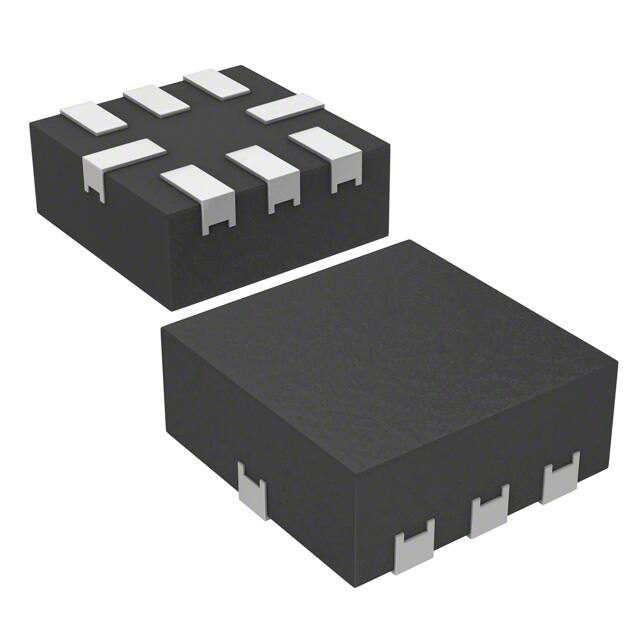
Ultra small miniQFN8 package of 1.4 x 1.4 x 0.55 mm
> 300 mA latch up current per JESD78
Switch exceeds 5 kV ESD/HBM
Combining low power, high speed, low on-resistance and
small physical size, the DG2737, DG2738, DG2739 are ideal
for portable and battery powered applications requiring high
performance and efficient use of board space.
The DG2737, DG2738, DG2739 come in a small miniQFN-8
lead package (1.4 x 1.4 x 0.55 mm). As a committed partner
to the community and the environment, Vishay Siliconix
manufactures this product with the lead (Pb)-free device
terminations and is 100 % RoHS compliant.
FUNCTIONAL BLOCK DIAGRAM AND PIN CONFIGURATION
DG2737
miniQFN-8L
V+
DG2738
miniQFN-8L
V+
8
DG2739
miniQFN-8L
V+
88
VIN
1
7
NC
S1
2
6
D1
3
5
88
VIN1
1
7
VIN2
S2
S1
2
6
D2
D1
3
5
48
VIN1
1
7
VIN2
S2
S1
2
6
S2
D2
D1
3
53
D2
48
48
GND
GND
GND
Top View
Top View
Top View
Ax
Bx
Cx
Pin 1
Pin 1
Pin 1
Device Marking: Ax for DG2737
x = Date/Lot Traceability Code
Device Marking: Bx for DG2738
x = Date/Lot Traceability Code
Device Marking: Cx for DG2739
x = Date/Lot Traceability Code
Document Number: 68801
S-82643-Rev. B, 03-Nov-08
www.vishay.com
1
�DG2737, DG2738, DG2739
Vishay Siliconix
TRUTH TABLE 1
Input
DG2737
Logic
VIN
S1 and D1
S2 and D2
Low
ON
ON
High
OFF
OFF
TRUTH TABLE 2
Input
VIN1
VIN2
Logic
DG2738
DG2739
S1 and D1
S2 and D2
S1 and D1
S2 and D2
Low
ON
High
OFF
X
ON
X
X
OFF
X
Low
X
ON
X
OFF
High
X
OFF
X
ON
ORDERING INFORMATION
Temp. Range
- 40 °C to 85°C
Package
Part Number
miniQFN-8L
DG2737DN-T1-E4
DG2738DN-T1-E4
DG2739DN-T1-E4
ABSOLUTE MAXIMUM RATINGS TA = 25 °C, unless otherwise noted
Parameter
Limit
- 0.3 to 5.0
- 0.3 to (V+ + 0.3)
30
± 300
± 500
- 65 to 150
190
V+
VIN, D, Sa
Reference to GND
Unit
V
Current (Any terminal except D or S)
mA
Continuous Current (D or S)
Peak Current (Pulsed at 1 ms, 10 % Duty Cycle)
Storage Temperature (D Suffix)
°C
Power Dissipation (Packages)b
miniQFN-8Lc
mW
Notes:
a. Signals on VIN, D, or S exceeding V+ will be clamped by internal diodes. Limit forward diode current to maximum current ratings.
b. All leads welded or soldered to PC board.
c. Derate 2.4 mW/°C above 70 °C.
SPECIFICATIONS V+ = 3 V
Parameter
Symbol
Test Conditions
Unless Otherwise Specified
V+ = 3 V, VIN = 0.4 V or 1.4 Ve
Vanalog
RON
Limits
- 40 °C to 85 °C
Temp.a
Min.b
Full
0
Typ.c
Max.b
Unit
V+
V
Analog Switch
Analog Signal Ranged
On-Resistance
RON Matchd
RON Flatnessd
www.vishay.com
2
Room
6
8
RON
V+ = 3 V, IS = 8 mA, VD = 0.4 V
ΔRON
V+ = 3 V, IS = 8 mA, VD = 0.4 V
Room
0.1
0.5
RON
Flatness
V+ = 3 V, IS = 8 mA,
VD = 0 V, 1 V
Room
2.6
4
Full
9
Ω
Document Number: 68801
S-82643-Rev. B, 03-Nov-08
�DG2737, DG2738, DG2739
Vishay Siliconix
SPECIFICATIONS V+ = 3 V
Parameter
Symbol
Test Conditions
Unless Otherwise Specified
V+ = 3 V, VIN = 0.4 V or 1.4 Ve
Limits
- 40 °C to 85 °C
Temp.a
Min.b
Typ.c
Max.b
Unit
Analog Switch
Switch Off Leakage
Current
Channel-On Leakage Current
IS(off)
ID(off)
ID(on)
V+ = 4.3 V, VS = 0.3 V/3.3 V,
VD = 3.3 V/0.3 V
V+ = 4.3 V, VS = VD = 4 V/0.3 V
Room
- 10
10
Full
- 100
100
Room
- 10
10
Full
- 100
100
Room
- 10
10
Full
- 100
100
Full
1.3
nA
Digital Control
Input High Voltage
VINH
Input Low Voltage
VINL
Input Current
IINL or IINH
V+ = 2.3 V to 4.3 V
VIN = 0 or V+
Full
Full
V
0.5
-1
1
µA
Dynamic Characteristics
Turn-On Timee
tON
Turn-Off Timee
tOFF
Break-Before-Make Time
Charge Injectiond
Off-Isolationd
Room
V+ = 2.3 V to 3.6 V, VNO or VS = 1.5 V,
RL = 50 Ω, CL = 35 pF
V+ = 2.3 V to 4.3 V
Q
CL = 1 nF, RGEN = 0 Ω, VGEN = 0 V
6
Room
10.4
RL = 50 Ω, CL = 5 pF, f = 10 MHz
- 59
dB
- 109
- 99
- 48
Room
720
Channel to Channel skewd
MHz
25
Skew of Opposite Transitions
of the Same Outputd
RL = 50 Ω, CL = 5 pF
Room
20
Total Jitterd
ps
200
Source Off Capacitanced
CS(off)
f = 1 MHz, VS = 0 V
Room
4.4
Drain Off Capacitanced
CD(off)
f = 1 MHz, VD = 0 V
Room
3.8
Drain On Capacitanced
CD(on)
f = 1 MHz, VD = VS = 0 V
Room
10
CIN
f = 1 MHz
Room
8.3
VIN = 0 or V+
Full
Control Pin Capacitanced
pC
- 28
Room
RL = 50 Ω, CL = 5 pF, f = 10 MHz
RL = 50 Ω, CL = 5 pF
ns
1
RL = 50 Ω, CL = 5 pF, f = 240 MHz
3 dB bandwidthd
ns
50
60
Room
- 79
RL = 50 Ω, CL = 5 pF, f = 1 MHz
XTALK
13
RL = 50 Ω, CL = 5 pF, f = 1 MHz
RL = 50 Ω, CL = 5 pF, f = 240 MHz
Crosstalkd
Room
Full
60
70
Full
tBBM
OIRR
23
Full
pF
Power Supply
Power Supply Range
V+
Power Supply Current
I+
2.3
4.3
V
1.0
µA
Notes:
a. Room = 25 °C, Full = as determined by the operating suffix.
b. The algebraic convention whereby the most negative value is a minimum and the most positive a maximum, is used in this data sheet.
c. Typical values are for design aid only, not guaranteed nor subject to production testing.
d. Guarantee by design, not subjected to production test.
e. VIN = input voltage to perform proper function.
Stresses beyond those listed under “Absolute Maximum Ratings” may cause permanent damage to the device. These are stress ratings only, and functional operation
of the device at these or any other conditions beyond those indicated in the operational sections of the specifications is not implied. Exposure to absolute maximum
rating conditions for extended periods may affect device reliability.
Document Number: 68801
S-82643-Rev. B, 03-Nov-08
www.vishay.com
3
�DG2737, DG2738, DG2739
Vishay Siliconix
TYPICAL CHARACTERISTICS 25 °C, unless otherwise noted
18
35
V+ = 2.3
2.3VV
16
30
+ 85 °C
14
R ON - On-Resistance (Ω)
R ON - On-Resistance (Ω)
V+ = 2.5 V
25
V+ = 2.7
2.7VV
20
V+
V+==3 3VV
V+ = 3.6 V
15
V+ = 4.3 V
10
12
+ 25 °C
10
8
- 40 °C
6
4
5
2
V+ = 3.0 V
0
0
0
1
2
3
4
0
5
0.5
2
2.5
3
4
5
VD - Analog Voltage (V)
VD - Analog Voltage (V)
RON vs. VD and Temperature
200
V+ = 4.3 V
V+ = + 4.3 V
75
150
70
100
Leakage Current (pA)
I+ - Supply Current (nA)
1.5
RON vs. VD and Supply Voltage
80
65
60
55
I D(OFF)
I D(ON)
50
0
- 50
50
- 100
45
- 150
40
- 60
1
I S(OFF)
- 200
- 40
- 20
0
20
40
60
80
100
0
1
2
Temperature (°C)
3
VD , VS - Analog Voltage (V)
Supply Current vs. Temperature
Leakage vs. Analog Voltage
16
10 000
V + = + 4.3 V
V+ = + 4.3 V
14
ID(OFF)
Q - Charge Injection (pC)
Leakage Current (pA)
1000
ID(ON)
100
10
IS(OFF)
1
- 60
10
8
V+ = + 3.6 V
6
V+ = + 3 V
4
V+ = + 2.3 V
2
C L =1 nF
Drain
V+ = + 2.7 V
0
- 40
- 20
0
20
40
60
80
Temperature (°C)
Leakage Current vs. Temperature
www.vishay.com
4
12
100
0
1
2
3
4
5
VD - Analog Voltage (V)
Charge Injection vs. Analog Voltage
Document Number: 68801
S-82643-Rev. B, 03-Nov-08
�DG2737, DG2738, DG2739
Vishay Siliconix
TYPICAL CHARACTERISTICS 25 °C, unless otherwise noted
1.3
35
V+ = 2.7 V
tON
1.2
- 40 °C to 85 °C
VT - Switching Threshold (V)
tON, tOFF - Switching Time (ns)
30
25
20
15
10
V+ = 2.7 V
tOFF
V+ = 3.6 V
tOFF
V+ = 3.6 V
tON
5
0
- 60
1.1
1.0
0.9
0.8
0.7
0.6
- 40
- 20
0
20
40
60
80
0.5
2.0
100
2.5
3.0
3.5
4.0
Temperature (°C)
V+ - Supply Voltage (V)
Switching Time vs. Temperature
Switching Threshold vs. Supply Voltage
0
4.5
0
- 10
- 20
-1
-2
OIRR, XTALK (dB)
Insertion Loss (dB)
- 30
-3
-4
- 40
OIRR
- 50
- 60
- 70
XTALK
- 80
- 90
- 100
V+ = 3 V
R L = 50 Ω
-5
-6
100K
1M
10M
100M
Frequency (Hz)
Insertion Loss vs. Frequency
Document Number: 68801
S-82643-Rev. B, 03-Nov-08
V+ = 3 V
RL = 50 Ω
- 110
- 120
1G
- 130
100K
1M
10M
100M
1G
Frequency (Hz)
Off-Isolation, Crosstalk vs. Frequency
www.vishay.com
5
�DG2737, DG2738, DG2739
Vishay Siliconix
TEST CIRCUITS
V+
Logic
Input
V+
S
Switch
Input
tr < 5 ns
tf < 5 ns
50 %
VINL
Switch Output
D
VINH
VOUT
0.9 x V OUT
Logic
Input
Switch
Output
VIN
RL
50 Ω
GND
CL
35 pF
0V
tON
tOFF
0V
Logic "1" = Switch On
Logic input waveforms inverted for switches that have
the opposite logic sense.
CL (includes fixture and stray capacitance)
VOUT = VD
(R L
RL
+ R
ON
)
Figure 1. Switching Time
V+
VINH
Logic
Input
VS2
V+
D2
S2
VO2
VIN2
VS1
Switch
Output
VIN1
RL2
50 Ω
GND
90 %
VO1
D1
S1
50 %
VINL
VS2
VO2
RL1
50 Ω
CL2
35 pF
CL1
35 pF
0V
VS1
VO1
0V
Switch
Output
90 %
tD
tD
CL (includes fixture and stray capacitance)
Figure 2. Break-Before-Make (DG2739)
ΔVO
V+
Rg
Vg
VIN = 0 - V+
VO
VINX
V+
S
VIN
OFF
D
ON
OFF
VO
CL
1 nF
GND
VINX
OFF
ON
Q = ΔVO x CL
OFF
Figure 3. Charge Injection
www.vishay.com
6
Document Number: 68801
S-82643-Rev. B, 03-Nov-08
�DG2737, DG2738, DG2739
Vishay Siliconix
TEST CIRCUITS
V+
V+
S
0 V, V+
VIN
D
RL
Analyzer
GND
VD
Off Isolation = 20 log V
S
Figure 4. Off-Isolation
V+
C
VS
V+
D1
S
Rg = 50 Ω
50 Ω
VIN1
0 V, V+
S2
0 V, V+
D2
VO
RL
VIN2
GND
XTALK Isolation = 20 log
VO
VS
C = RF bypass
Figure 5. Crosstalk
V+
V+
D
Meter
IN
0 V, V+
S
HP4192A
Impedance
Analyzer
or Equivalent
GND
f = 1 MHz
Figure 6. Channel Off/On Capacitance
Vishay Siliconix maintains worldwide manufacturing capability. Products may be manufactured at one of several qualified locations. Reliability data for Silicon
Technology and Package Reliability represent a composite of all qualified locations. For related documents such as package/tape drawings, part marking, and
reliability data, see http://www.vishay.com/ppg?68801.
Document Number: 68801
S-82643-Rev. B, 03-Nov-08
www.vishay.com
7
�Package Information
Vishay Siliconix
MINIQFN-8L CASE OUTLINE
A
D
6
5
5
6
7
L
7
b
4
8
4
E
8
L
L
L
1
2
3
3
2
1
A
A1
c
e
MILLIMETERS
INCHES
DIM
MIN.
NOM.
MAX.
MIN.
NOM.
MAX.
A
0.50
0.55
0.60
0.0197
0.0217
0.0236
A1
0.00
-
0.05
0.000
-
0.002
b
0.15
0.20
0.25
0.006
0.008
0.010
c
0.15 REF
0.006 REF
D
1.35
1.40
1.45
0.053
0.055
0.057
E
1.35
1.40
1.45
0.053
0.055
0.057
e
L
0.40 BSC
0.35
0.40
0.016 BSC
0.45
0.014
0.016
0.018
ECN: C-08336-Rev. A, 05-May-08
DWG: 5964
Document Number: 68674
Revision: 05-May-08
www.vishay.com
1
�PAD Pattern
Vishay Siliconix
RECOMMENDED MINIMUM PADS FOR MINI QFN 8L
1.70
0.80
1.70
0.60
x6
0.125
typ. 0.25
x2
0.50
0.40
0.25
x6
Suggested Minimum Pad
Dimensions in mm
Document Number: 66555
Revision: 05-Mar-10
www.vishay.com
1
�Legal Disclaimer Notice
www.vishay.com
Vishay
Disclaimer
ALL PRODUCT, PRODUCT SPECIFICATIONS AND DATA ARE SUBJECT TO CHANGE WITHOUT NOTICE TO IMPROVE
RELIABILITY, FUNCTION OR DESIGN OR OTHERWISE.
Vishay Intertechnology, Inc., its affiliates, agents, and employees, and all persons acting on its or their behalf (collectively,
“Vishay”), disclaim any and all liability for any errors, inaccuracies or incompleteness contained in any datasheet or in any other
disclosure relating to any product.
Vishay makes no warranty, representation or guarantee regarding the suitability of the products for any particular purpose or
the continuing production of any product. To the maximum extent permitted by applicable law, Vishay disclaims (i) any and all
liability arising out of the application or use of any product, (ii) any and all liability, including without limitation special,
consequential or incidental damages, and (iii) any and all implied warranties, including warranties of fitness for particular
purpose, non-infringement and merchantability.
Statements regarding the suitability of products for certain types of applications are based on Vishay’s knowledge of typical
requirements that are often placed on Vishay products in generic applications. Such statements are not binding statements
about the suitability of products for a particular application. It is the customer’s responsibility to validate that a particular
product with the properties described in the product specification is suitable for use in a particular application. Parameters
provided in datasheets and/or specifications may vary in different applications and performance may vary over time. All
operating parameters, including typical parameters, must be validated for each customer application by the customer’s
technical experts. Product specifications do not expand or otherwise modify Vishay’s terms and conditions of purchase,
including but not limited to the warranty expressed therein.
Except as expressly indicated in writing, Vishay products are not designed for use in medical, life-saving, or life-sustaining
applications or for any other application in which the failure of the Vishay product could result in personal injury or death.
Customers using or selling Vishay products not expressly indicated for use in such applications do so at their own risk. Please
contact authorized Vishay personnel to obtain written terms and conditions regarding products designed for such applications.
No license, express or implied, by estoppel or otherwise, to any intellectual property rights is granted by this document or by
any conduct of Vishay. Product names and markings noted herein may be trademarks of their respective owners.
Material Category Policy
Vishay Intertechnology, Inc. hereby certifies that all its products that are identified as RoHS-Compliant fulfill the
definitions and restrictions defined under Directive 2011/65/EU of The European Parliament and of the Council
of June 8, 2011 on the restriction of the use of certain hazardous substances in electrical and electronic equipment
(EEE) - recast, unless otherwise specified as non-compliant.
Please note that some Vishay documentation may still make reference to RoHS Directive 2002/95/EC. We confirm that
all the products identified as being compliant to Directive 2002/95/EC conform to Directive 2011/65/EU.
Vishay Intertechnology, Inc. hereby certifies that all its products that are identified as Halogen-Free follow Halogen-Free
requirements as per JEDEC JS709A standards. Please note that some Vishay documentation may still make reference
to the IEC 61249-2-21 definition. We confirm that all the products identified as being compliant to IEC 61249-2-21
conform to JEDEC JS709A standards.
Revision: 02-Oct-12
1
Document Number: 91000
�


 工商网监
湘ICP备2023018690号
工商网监
湘ICP备2023018690号
