DG2799
Vishay Siliconix
Low Voltage, Low On-Resistance, Dual DPDT Analog Switch
DESCRIPTION
The DG2799 is a dual double-pole/double-throw monolithic
CMOS analog switch designed for high performance switching of analog signals. Combining low power, high speed, low
on-resistance and small physical size, the DG2799 is ideal
for portable and battery powered applications requiring high
performance and efficient use of board space.
The DG2799 is built on Vishay Siliconix’s low voltage process. An epitaxial layer prevents latchup. Break-beforemake is guaranteed.
The switch conducts equally well in both directions when on,
and blocks up to the power supply level when off.
As a committed partner to the community and the environment, Vishay Siliconix manufactures this product with the
lead (Pb)-free device terminations. For analog switching
products manufactured in QFN packages, the lead (Pb)-free
“-E3/E4” only suffix is being used as a designator. Lead (Pb)free QFN products purchased at any time will have either a
nickel-palladium-gold device termination or a 100 % matte
tin device termination. The different lead (Pb)-free materials
are interchangeable and meet all JEDEC standards for
reflow and MSL rating.
FEATURES
• Low Voltage Operation (1.65 V to 4.3 V)
• Low On-Resistance - rON: 0.25 Ω @ 2.7 V
• Fast Switching: tON = 28 ns
tOFF = 17 ns
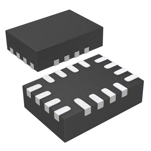
• QFN-16 (3 x 3) Package
• Latch-Up Current > 300 mA (JESD78)
BENEFITS
• Reduced Power Consumption
• High Accuracy
• Reduce Board Space
• TTL/1.8-V Logic Compatible
• High Bandwidth
APPLICATIONS
• Cellular Phones
• Speaker Headset Switching
• Audio and Video Signal Routing
• PCMCIA Cards
• Battery Operated Systems
FUNCTIONAL BLOCK DIAGRAM AND PIN CONFIGURATION
DG2799
QFN-16 (3 X 3)
COM1 NO1
16
15
V+
14
TRUTH TABLE
NC4
Logic
NC1, 2, 3 and 4
NO1, 2, 3 and 4
13
0
ON
OFF
1
OFF
ON
NC1
1
12
COM4
IN1, IN2
2
11
NO4
NO2
3
10
IN3, IN4
COM2
4
9
5
6
NC2
GND
7
NC3
ORDERING INFORMATION
Temp Range
Package
Part Number
–40 to 85°C
16-Pin QFN (3 x 3 mm)
Variation 2
DG2799DN-T1—E4
8
NO3 COM3
Top View
NOTE:
Underside exposed pad has no device electrical connection. It is recommended that no electrical connection is made to it.
Document Number: 72922
S-52336–Rev. F, 07-Nov-05
www.vishay.com
1
�DG2799
Vishay Siliconix
ABSOLUTE MAXIMUM RATINGS TA = 25 °C, unless otherwise noted
Parameter
Symbol
Limit
–0.3 to 5.0
–0.3 to (V+ + 0.3)
30
±300
±500
–65 to 150
250
1385
V+
Reference to GND
IN, COM, NC, NOa
Current (Any terminal except NO, NC or COM)
Continuous Current (NO, NC, or COM)
Peak Current (Pulsed at 1 ms, 10 % duty cycle)
Storage Temperature (D Suffix)
16-Pin QFN (3 x 3 mm)
Package Solder Reflow Conditionsd
Unit
V
mA
°C
mW
QFN-16c
Power Dissipation (Packages)b
Notes
a. Signals on NC, NO, or COM or IN exceeding V+ will be clamped by internal diodes. Limit forward diode current to maximum current ratings.
b. All leads welded or soldered to PC Board.
c. Derate 17.3 mW/°C above 70°C
d. Manual soldering with iron is not recommended for leadless components. The QFN is a leadless package. The end of the lead terminal is
exposed copper (not plated) as a result of the singulation process in manufacturing. A solder fillet at the exposed copper lip cannot be guaranteed
and is not required to ensure adequate bottom side solder interconnection.
SPECIFICATIONS (V+ = 1.8 V)
Limits
–40 to 85°C
Test Condition
Otherwise Unless Specified
Parameter
Symbol
V+ = 1.8 V, VIN = 0.4 or 1.1 Ve
Tempa
Minb
Full
0
Typc
Maxb
Unit
V+
V
1.3
Ω
Analog Switch
Analog Signal Ranged
VNO, VNC,
VCOM
V+ = 1.8 V, VCOM = 0.2 V, INO, INC = 100 mA
rON
On-Resistance
V+ = 1.8 V, VCOM = 0.9 V, INO, INC = 100 mA
0.35
Room
0.45
Full
1.4
Digital Control
Input High Voltage
VINH
Full
Input Low Voltage
VINL
Full
Input Capacitance
Input Current
Cin
IINL or IINH
1.1
0.4
Full
VIN = 0 or V+
Full
pF
6
–1
V
1
µA
Dynamic Characteristics
Turn-On Time
tON
Turn-Off Time
tOFF
Break-Before-Make Time
Charge Injection
d
OIRR
Crosstalkd
XTALK
NO, NC Off Capacitanced
Channel-On Capacitanced
62
94
97
VNO or VNC = 1.5 V, RL = 50 Ω, CL = 35 pF
Room
Full
24
52
55
CL = 1 nF, VGEN = 0 V, RGEN = 0 Ω
Room
td
QINJ
Off-Isolation
d
Romm
Full
Full
8
66
Room
–74
Room
–74
CNO(off)
Room
108
CNC(off)
Room
108
Room
240
Room
240
CNO(on)
RL = 50 Ω, CL = 5 pF, f = 100 kHz
VIN = 0 or V+, f = 1 MHz
CNC(on)
ns
pC
dB
pF
Power Supply
Power Supply Current
www.vishay.com
2
I+
VIN = 0 or V+
Full
1.0
µA
Document Number: 72922
S-52336–Rev. F, 07-Nov-05
�DG2799
Vishay Siliconix
SPECIFICATIONS (V+ = 3 V)
Limits
–40 to 85°C
Test Condition
Otherwise Unless Specified
Parameter
Symbol
V+ = 3 V, ±10 %, VIN = 0.5 or 1.4 Ve
Tempa
Minb
Full
0
Typc
Maxb
Unit
V+
V
Analog Switch
VNO, VNC,
VCOM
Analog Signal Ranged
V+ = 2.7 V, VCOM = 0.2 V, INO, INC = 100 mA
On-Resistance
rON
rON Flatnessd
rON
Flatness
V+ = 2.7 V, VCOM = 1.5 V, INO, INC = 100 mA
0.3
Room
0.25
Full
∆rON
rON Matchd
Switch Off Leakage Current
INO(off),
INC(offF)
ICOM(off)
Channel-On Leakage
Current
ICOM(on)
V+ = 2.7 V, VCOM = 0 to V+,
INO, INC = 100 mA
V+ = 3.3 V, VNO, VNC = 0.3 V / 3.0 V,
VCOM = 3.0 V / 0.3 V
V+ = 3.3 V, VNO, VNC = VCOM = 0.3 V / 3.0 V
0.45
0.55
Room
0.07
Room
0.05
Ω
0.15
Room
Full
–1
–10
1
10
Room
Full
–1
–10
1
10
Room
Full
–1
–10
1
10
1.4
nA
Digital Control
Input High Voltage
VINH
Full
Input Low Voltage
VINL
Full
Input Capacitance
Cin
Full
Input Current
IINL or IINH
VIN = 0 or V+
Full
0.5
pF
6
–1
V
1
µA
Dynamic Characteristics
Romm
Full
28
57
60
VNO or VNC = 1.5 V, RL = 50 Ω, CL = 35 pF
Room
Full
17
45
47
CL = 1 nF, VGEN = 0 V, RGEN = 0 Ω
Room
160
Room
–75
Room
–75
CNO(off)
Room
102
CNC(off)
Room
102
Room
234
Room
234
Turn-On Time
tON
Turn-Off Time
tOFF
Break-Before-Make Time
td
Injectiond
QINJ
d
OIRR
Charge
Off-Isolation
XTALK
Crosstalkd
NO, NC Off Capacitanced
Channel-On Capacitance
d
CNO(on)
Full
RL = 50 Ω, CL = 5 pF, f = 100 kHz
VIN = 0 or V+, f = 1 MHz
CNC(on)
ns
1
pC
dB
pF
Power Supply
Power Supply Range
V+
Power Supply Current
I+
Document Number: 72922
S-52336–Rev. F, 07-Nov-05
2.7
VIN = 0 or V+
Full
3.3
V
1.0
µA
www.vishay.com
3
�DG2799
Vishay Siliconix
SPECIFICATIONS (V+ = 4.3 V)
Limits
–40 to 85°C
Test Condition
Otherwise Unless Specified
Parameter
Symbol
V+ = 4.3 V, VIN = 0.5 or 1.6 Ve
Tempa
Minb
Full
0
Typc
Maxb
Unit
V+
V
Analog Switch
VNO, VNC,
VCOM
Analog Signal Ranged
V+ = 4.3 V, VCOM = 0.5 V, INO, INC = 100 mA
On-Resistance
rON
rON Flatnessd
rON
Flatness
V+ = 4.3 V, VCOM = 2.1 V, INO, INC = 100 mA
0.29
Room
0.21
Full
∆rON
rON Matchd
INO(off),
INC(offF)
Switch Off Leakage
Currentd
ICOM(off)
Channel-On Leakage
ICOM(on)
Currentd
V+ = 4.3 V, VCOM = 0 to V+,
INO, INC = 100 mA
V+ = 4.3 V, VNO, VNC = 0.3 V / 4.0 V,
VCOM = 4.0 V / 0.3 V
V+ = 4.3 V, VNO, VNC = VCOM = 3.0 V / 4.0 V
0.43
0.53
Room
0.07
Room
0.05
Ω
0.15
Room
Full
–10
–100
10
100
Room
Full
–10
–100
10
100
Room
Full
–10
–100
10
100
1.6
nA
Digital Control
Input High Voltage
VINH
Full
Input Low Voltage
VINL
Full
Input Capacitance
Cin
Full
Input Current
IINL or IINH
VIN = 0 or V+
Full
QINJ
CL = 1 nF, VGEN = 0 V, RGEN = 0 Ω
Room
V
0.5
pF
6
–1
1
µA
Dynamic Characteristics
Charge Injectiond
OIRR
Off-Isolationd
Crosstalk
NO, NC Off Capacitanced
Channel-On Capacitance
Room
–73
Room
–73
CNO(off)
Room
100
CNC(off)
Room
100
Room
230
Room
230
XTALK
d
d
320
CNO(on)
RL = 50 Ω, CL = 5 pF, f = 100 kHz
VIN = 0 or V+, f = 1 MHz
CNC(on)
pC
dB
pF
Power Supply
Power Supply Range
V+
Power Supply Current
I+
VIN = 0 or V+
Full
4.3
V
1.0
µA
Notes
a. Room = 25°C, Full = as determined by the operating suffix.
b. The algebraic convention whereby the most negative value is a minimum and the most positive a maximum, is used in this data sheet.
c. Typical values are for design aid only, not guaranteed nor subject to production testing.
d. Guarantee by design, not subjected to production test.
e. VIN = input voltage to perform proper function.
Stresses beyond those listed under “Absolute Maximum Ratings” may cause permanent damage to the device. These are stress ratings only, and functional operation
of the device at these or any other conditions beyond those indicated in the operational sections of the specifications is not implied. Exposure to absolute maximum
rating conditions for extended periods may affect device reliability.
www.vishay.com
4
Document Number: 72922
S-52336–Rev. F, 07-Nov-05
�DG2799
Vishay Siliconix
TYPICAL CHARACTERISTICS
TA = 25 °C, unless otherwise noted
0.8
0.8
V+ = 1.65 V
T = 25˚C
IS = 100 mA
NC Switch
V+ = 1.8 V
0.6
V+ = 2.0 V
0.5
V+ = 2.3 V
V+ = 2.7 V
0.4
V+ = 3.0 V
0.3
0.2
V+ = 3.3 V
0.1
0.0
0.0
0.5
1.0
1.5
VCOM
2.0
2.5
V+ = 3.6 V
3.0
3.5
IS = 100 mA
V+ = 3 V
0.7
r ON - On-Resistance ( Ω )
r ON - On-Resistance ( Ω )
0.7
0.6
85˚C
0.5
25˚C
0.4
-40°C
0.3
0.2
0.1
0.0
0.0
4.0
1.0
1.5
Analog Voltage (V)
2.0
2.5
3.0
Analog Voltage (V)
VCOM
rON vs. VCOM and Supply Voltage
rON vs. Analog Voltage and Temperature
0.6
10000
IS = 100 mA
V+ = 4.3 V
0.5
V+ = 3 V
VIN = 0 V
1000
85˚C
0.4
I+ - Supply Current (nA)
r ON - On-Resistance ( Ω )
0.5
25˚C
-40°C
0.3
0.2
100
10
0.1
0.0
1
0
1
2
VCOM
3
4
5
-60
-40
-20
0
20
40
60
80
10
Temperature ( ˚C)
Analog Voltage (V)
rON vs. Analog Voltage and Temperature
Supply Current vs. Temperature
1000
100 mA
V+ = 3.3 V
V+ = 2.7 V
Leakage Current (pA)
I+ - Supply Current (A)
10 mA
1 mA
100 µA
10 µA
1 µA
100 nA
INO(off), INC(off)
100
ICOM(off)
ICOM(on)
10
10 nA
1 nA
1
-60
100 pA
10
100
1K
10 K
100 K
1M
10 M
-40
-20
0
20
40
60
80
10
Temperature ( ˚C)
Input Switching Frequency (Hz)
Supply Current vs. Input Switching Frequency
Document Number: 72922
S-52336–Rev. F, 07-Nov-05
Supply Current vs. Temperature
www.vishay.com
5
�DG2799
Vishay Siliconix
TYPICAL CHARACTERISTICS TA = 25 °C, unless otherwise noted
300
70
tON V+ = 1.8 V
250
ICOM(off)
150
INO(off), IINC(off)
100
50
0
50
ICOM(on)
-100
60
t ON / t OFF - Switching Time (µs)
Leakage Current (pA)
200
V+ = 3.3 V
-150
-200
50
tON V+ = 2.3 V
40
tON V+ = 3.0 V
30
20
tOFF V+ = 1.8 V
10
-250
-300
0.00
tOFF V+ = 2.3 V
0
0.50
1.00
1.50
VCOM, VNO, VNC
2.00
2.50
3.00
-60
-40
0
20
40
60
80
100
Temperature (˚C)
Leakage vs. Analog Voltage
Switching Time vs. Temperature
10
2.00
1.75
- Switching Threshold (V)
LOSS
-10
XTALK
-30
OIRR
-50
V+ = 3 V
RL = 50Ω
-70
1.50
1.25
1.00
0.75
0.50
VT
Loss, OIRR, X TALK (dB)
-20
Analog Voltage (V)
tOFF V+ = 3.0 V
0.25
-90
100 K
1M
100 M
10 M
0.00
1.0
1G
1.5
2.0
Frequency (Hz)
2.5
V+
Insertion Loss, Off-Isolation
Crosstalk vs. Frequency
3.0
3.5
4.0
4.5
5.0
Supply Voltage (V)
ISwitching Threshold vs. Supply Voltage
150
100
V+ = 1.8 V
V+ = 3 V
Q - Charge Injection (pC)
50
0
50
V+ = 4.3 V
100
150
200
250
300
350
0.0
0.5
1.0
1.5
2.0
2.5
3.0
3.5
4.0
4.5
VCOM - Analog Voltage (V)
Charge Injection vs. Analog Voltage
www.vishay.com
6
Document Number: 72922
S-52336–Rev. F, 07-Nov-05
�DG2799
Vishay Siliconix
TEST CIRCUITS
V+
VINH
Logic
Input
V+
NO or NC
Switch
Input
VINL
Switch Output
COM
tr < 5 ns
tf < 5 ns
50%
VOUT
0.9 x VOUT
Logic
Input
Switch
Output
IN
RL
50 Ω
GND
CL
35 pF
0V
tON
tOFF
0V
Logic “1” = Switch On
Logic input waveforms inverted for switches that have
the opposite logic sense.
CL (includes fixture and stray capacitance)
VOUT = VCOM
(R L
RL
+ R
ON
)
Figure 1. Switching Time
V+
Logic
Input
V+
COM
NO
VNO
VINH
tr < 5 ns
tf < 5 ns
VINL
VO
NC
VNC
RL
50Ω
IN
CL
35 pF
GND
VNC = VNO
VO
90%
Switch
0V
Output
tD
tD
CL (includes fixture and stray capacitance)
Figure 2. Break-Before-Make Interval
V+
Rgen
∆ VOUT
V+
NC or NO
COM
VOUT
VOUT
+
IN
IN
Vgen
CL = 1 nF
VIN = 0 - V+
On
Off
On
GND
Q = ∆VOUT x CL
IN depends on switch configuration: input polarity
determined by sense of switch.
Figure 3. Charge Injection
Document Number: 72922
S-52336–Rev. F, 07-Nov-05
www.vishay.com
7
�DG2799
Vishay Siliconix
TEST CIRCUITS
V+
V+
10 nF
10 nF
V+
V+
NC or NO
IN
COM
COM
0V, 2.4 V
Meter
COM
IN
0 V, 2.4 V
RL
NC or NO
GND
HP4192A
Impedance
Analyzer
or Equivalent
GND
Analyzer
f = 1 MHz
VCOM
Off Isolation = 20 log V
NO / NC
Figure 4. Off-Isolation
Figure 5. Channel Off/On Capacitance
Vishay Siliconix maintains worldwide manufacturing capability. Products may be manufactured at one of several qualified locations. Reliability data for Silicon Technology and Package Reliability represent a composite of all qualified locations. For related documents such as package/tape drawings, part marking, and reliability
data, see http://www.vishay.com/ppg?72922.
www.vishay.com
8
Document Number: 72922
S-52336–Rev. F, 07-Nov-05
�Legal Disclaimer Notice
Vishay
Notice
Specifications of the products displayed herein are subject to change without notice. Vishay Intertechnology, Inc.,
or anyone on its behalf, assumes no responsibility or liability for any errors or inaccuracies.
Information contained herein is intended to provide a product description only. No license, express or implied, by
estoppel or otherwise, to any intellectual property rights is granted by this document. Except as provided in Vishay's
terms and conditions of sale for such products, Vishay assumes no liability whatsoever, and disclaims any express
or implied warranty, relating to sale and/or use of Vishay products including liability or warranties relating to fitness
for a particular purpose, merchantability, or infringement of any patent, copyright, or other intellectual property right.
The products shown herein are not designed for use in medical, life-saving, or life-sustaining applications.
Customers using or selling these products for use in such applications do so at their own risk and agree to fully
indemnify Vishay for any damages resulting from such improper use or sale.
Document Number: 91000
Revision: 08-Apr-05
www.vishay.com
1
�Legal Disclaimer Notice
Vishay
Disclaimer
All product specifications and data are subject to change without notice.
Vishay Intertechnology, Inc., its affiliates, agents, and employees, and all persons acting on its or their behalf
(collectively, “Vishay”), disclaim any and all liability for any errors, inaccuracies or incompleteness contained herein
or in any other disclosure relating to any product.
Vishay disclaims any and all liability arising out of the use or application of any product described herein or of any
information provided herein to the maximum extent permitted by law. The product specifications do not expand or
otherwise modify Vishay’s terms and conditions of purchase, including but not limited to the warranty expressed
therein, which apply to these products.
No license, express or implied, by estoppel or otherwise, to any intellectual property rights is granted by this
document or by any conduct of Vishay.
The products shown herein are not designed for use in medical, life-saving, or life-sustaining applications unless
otherwise expressly indicated. Customers using or selling Vishay products not expressly indicated for use in such
applications do so entirely at their own risk and agree to fully indemnify Vishay for any damages arising or resulting
from such use or sale. Please contact authorized Vishay personnel to obtain written terms and conditions regarding
products designed for such applications.
Product names and markings noted herein may be trademarks of their respective owners.
Document Number: 91000
Revision: 18-Jul-08
www.vishay.com
1
�


 工商网监
湘ICP备2023018690号
工商网监
湘ICP备2023018690号
