DG3157A, DG3157B
Vishay Siliconix
Low Voltage, 300-MHz - 3 dB Bandwidth, SPDT Analog Switch with
Power Down Protection
(2:1 Multiplexer/Demultiplexer Bus Switch)
DESCRIPTION
FEATURES
The DG3157A, DG3157B are high-speed single-pole
double-throw, low voltage switch. Using sub-micro CMOS
technology, the DG3157A, DG3157B achieves low onresistance and negligible propagation delay. The DG3157A,
DG3157B can handle both analog and digital signals and
permits signals with amplitudes of up to VCC to be
transmitted in either direction. Select pin of control logic input
can be over the V+. When the select pin is low, B0 is
connected to the output A pin. When the select pin is high,
B1 is connected to the output A pin. The path that is open will
have a high-impedance state with respect to the output A pin.
Break before make is guaranteed. The DG3157A has an
internal pull down resistor on the control pin S, while the
DG3157B does not.
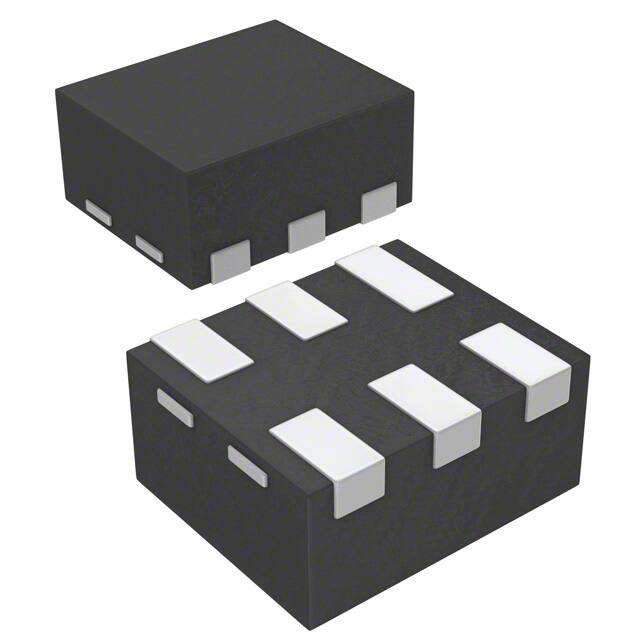
• Ultra small miniQFN6 package of
1 mm x 1.2 mm
Pb-free
• Wide operation voltage range: 1.8 V to 5.5 V
• Useful in both analog and digital signal
switching
Available
RoHS*
COMPLIANT
• 300 MHz - 3 dB bandwidth
• Power down safe design
• Low voltage logic threshold:
Vth(high) = 1.2 V at V+ = 3.3 V
• Minimal propagation delay
• Break-before-make switching
• Zero bounce in flow-through mode
• > 300 mA latch up current per JESD78
• > 8 kV ESD/HBM
• DG3157A version has internal pull down resistor on
control pin S
FUNCTIONAL BLOCK DIAGRAM AND PIN CONFIGURATION
miniQFN-6
DG3157A
TRUTH TABLE
1
B1
6
S
GND
2
5
V+
B0
3
4
A
Top View
Device Marking: E
miniQFN-6
DG3157B
B1
1
6
S
GND
2
5
V+
B0
3
4
A
Logic Input (S)
Function
0
B0 Connected to A
1
B1 Connected to A
ORDERING INFORMATION
Temp. Range
Package
- 40 °C to 85 °C
miniQFN-6
Part Number
DG3157ADN-T1-E4
DG3157BDN-T1-E4
Top View
Device Marking: D
* Pb containing terminations are not RoHS compliant, exemptions may apply.
Document Number: 68628
S-81944-Rev. C, 25-Aug-08
www.vishay.com
1
�DG3157A, DG3157B
Vishay Siliconix
ABSOLUTE MAXIMUM RATINGS
Parameter
Limit
Reference V+ to GND
Unit
- 0.3 to + 6
S, A, Ba
V
- 0.3 to (V+ + 0.3)
Continuous Current (Any terminal)
± 50
Peak Current (Pulsed at 1 ms, 10 % duty cycle)
± 200
Storage Temperature
D-Suffix
Power Dissipation (Packages)b
miniQFN-6c
mA
- 65 to 150
°C
160
mW
Notes:
a. Signals on A, or B or S exceeding V+ will be clamped by internal diodes. Limit forward diode current to maximum current ratings.
b. All leads welded or soldered to PC board.
c. Derate 2.0 mW/°C above 70 °C.
SPECIFICATIONS
Test Conditions
Unless Otherwise Specified
Parameter
DC Characteristics
High Level Input Voltage
Symbol
V+ = 3.0 V, VSL = 0.5 V, VSH = 2.0 Ve
Temp.a
Min.b
V+ = 1.65 to 1.95 V
1.2
V+ = 2.0 to 2.6 V
1.4
V+ = 2.7 to 3.6 V
2.0
VSH
V+ = 4.5 to 5.5 V
V+ = 1.65 to 1.95 V
Low Level Input Voltage
Limits
- 40 °C to 85 °C
VSL
Full
0.3
V+ = 2.0 to 2.6 V
0.4
V+ = 2.7 to 3.6 V
0.5
V+ = 4.5 V
RON
V+ = 3.0 V
V+ = 2.3 V
V+ = 1.65 V
On-Resistance Flatness
RFLAT
0 < VBN < V+
7
VBN = 2.4 V, IA = - 30 mA
5.7
12
VBN = 4.5 V, IA = - 30 mA
10.3
15
VBN = 0 V, IA = 24 mA
5.9
9
13.7
20
VBN = 3.0 V, IA = - 24 mA
Input Leakage Current
ΔRON
IS
VBN = 0 V, IA = 8 mA
7
12
16.2
30
VBN = 0 V, IA = 4 mA
9.2
20
VBN = 1.65 V, IA = - 4 mA
24
50
V+ = 4.5 V, IA = - 30 mA
8
V+ = 3.0 V, IA = - 24 mA
13
V+ = 2.3 V, IA = - 8 mA
24
Ω
0.8
0.1
V+ = 2.3 V, VBN = 1.6 V, IA = - 8 mA
0.2
V+ = 1.65 V, VBN = 1.15 V, IA = - 4 mA
0.9
V+ = 5.5 V,
VA = 5.5 V,
VS = 0.8 V, 2.4 V
V
89
Room
V+ = 3.0 V, VBN = 2.1 V, IA = - 24 mA
DG3157B
- 1.0
1.0
Full
DG3157A
Off Stage Switch Leakage
IBN(off)
V+ = 5.5 V, VA/VB = 0 V/5.5 V
On State Switch Leakage
IBN(on)
V+ = 5.5 V, VA/VB = 0 V/5.5 V
www.vishay.com
2
Full
VBN = 2.3 V, IA = - 8 mA
V+ = 1.65 V, IA = - 4 mA
Unit
0.8
4.8
V+ = 4.5 V, VBN = 3.15 V, IA = - 30 mA
On-Resistance Matching
Between Channels
Max.b
2.4
V+ = 4.5 to 5.5 V
VBN = 0 V, IA = 30 mA
On-Resistance
Typ.c
- 1.0
Room
Full
Room
Full
- 0.1
- 1.0
- 0.1
- 1.0
2.5
7.0
0.1
1.0
0.1
1.0
µA
Document Number: 68628
S-81944-Rev. C, 25-Aug-08
�DG3157A, DG3157B
Vishay Siliconix
SPECIFICATIONS
Test Conditions
Unless Otherwise Specified
Parameter
Power Supply
Power Supply Range
Symbol
V+ = 3.0 V, VSL = 0.5 V, VSH = 2.0 Ve
V+
Quiescent Supply Current
I+
V+ = 5.5 V, VA = V+ or GND
Limits
- 40 °C to 85 °C
Temp.a
Min.b
Full
Room
Full
1.65
Typ.c
Max.b
Unit
5.5
1
10
V
µA
AC Electrical Characteristice
Prop Delay Timef
tPHL/tPLH
V+ = 1.65 to 1.95 V
Full
1.5
V+ = 2.3 to 2.7 V
Full
0.8
V+ = 3.0 to 3.6 V
Full
0.4
V+ = 4.5 to 5.5 V
0.3
27
50
15
45
10
30
7
25
16
45
10
40
8
35
6
21
V+ = 1.65 to 1.95 V
Full
Room
Full
Room
Full
Room
Full
Room
Full
Room
Full
Room
Full
Room
Full
Room
Full
Full
0.5
11
V+ = 2.3 to 2.7 V
Full
0.5
6
V+ = 3.0 to 3.65
Full
0.5
4
Full
0.5
3
VA = 0 V
V+ = 1.65 to 1.95 V
Output Enable Time
f
tPZL/tPZH
VLOAD = 2 x V+ for tPZL
VLOAD = 0 V for tPZH
V+ = 2.3 to 2.7 V
V+ = 3.0 to 3.6 V
V+ = 4.5 to 5.5 V
V+ = 1.65 to 1.95 V
Output Disable
Timef
tPLZ/tPHZ
VLOAD = 2 x V+ for tPLZ
VLOAD = 0 V for tPHZ
V+ = 2.3 to 2.7 V
V+ = 3.0 to 3.6 V
V+ = 4.5 to 5.5 V
Break-Before-Make Timed
Charge Injectiond
Q
Off Isolationd
Crosstalk
tBBM
OIRR
d
XTALK
V+ = 4.5 to 5.5 V
CL = 1 nF, VGEN = 0 V
V+ = 5 V
RGEN = 0 Ω
V+ = 3.3 V
Room
7
Room
5
RL = 50 Ω, f = 10 MHz
Room
- 57
Room
- 64
ns
pC
dB
- 3 dB Bandwidthd
BW
RL = 50 Ω
Room
300
MHz
Total Harmonic Distortiond
Capacitance
THD
RL = 600 Ω, 0.5 Vp-p f = 600 Hz - 20 kHz
Room
0.016
%
CS
V+ = 0 V
Room
3.7
Room
7
Room
19
Control Pin Capacitanced
d
B Port Off Capacitance
A Port Capacitance When
CIO-B
CIO-A(on)
V+ = 5 V
pF
Switch Enabled
Notes:
a. Room = 25 °C, Full = as determined by the operating suffix.
b. The algebraic convention whereby the most negative value is a minimum and the most positive a maximum, is used in this data sheet.
c. Typical values are for design aid only, not guaranteed nor subject to production testing.
d. Guarantee by design, nor subjected to production test.
e. VS = input voltage to perform proper function.
f. Guaranteed by design and not production tested. The bus switch propagation delay is a function of the RC time constant contributed by the
on-resistance and the specified load capacitance with an ideal voltage source (zero output impedance) driving the switch.
Stresses beyond those listed under “Absolute Maximum Ratings” may cause permanent damage to the device. These are stress ratings only, and functional operation
of the device at these or any other conditions beyond those indicated in the operational sections of the specifications is not implied. Exposure to absolute maximum
rating conditions for extended periods may affect device reliability.
Document Number: 68628
S-81944-Rev. C, 25-Aug-08
www.vishay.com
3
�DG3157A, DG3157B
Vishay Siliconix
LOGIC DIAGRAM Positive Logic
B1
S
B0
1
6
4
A
3
Figure 1.
AC LOADING AND WAVEFORMS
VLD
RL
500 Ω
SW
Open
From Output
Under Test
GND
RL
500 Ω
CL
50 pF
TEST
SW
tPLH/tPHL
Open
tPLZ/tPZL
VLD
tPHZ/tPZH
GND
Load Circuit
Figure 2. AC Test Circuit
tf = 2.5 ns
tr = 2.5 ns
V+
90 %
Switch
Input
tr = 2.5 ns
tf = 2.5 ns
90 %
50 %
90 %
Logic
Input
50 %
50 %
50 %
10 %
10 %
10 %
GND
tPLZ
tPHL
tPLH
VOH
Output
10 %
tPZL
GND
tw
V+
90 %
50 %
50 %
Output
VOL + 0.3 V
Waveform 1
SW at V LD
50 %
VLD
2
VOL
tPZH
tPHZ
VOH
VOL
VOH 0.3 V
Output
Waveform 2
SW at GND
Propagation Delay T imes
50 %
0V
Enable and Disable T ime-Low- and High-Level Enabling
Figure 3. AC Waveforms
Notes:
• CL includes probe and jig capacitance.
• Waveform 1 is for an output with internal conditions such that the output is low except when disabled by the output control.
• Waveform 2 is for an output with internal conditions such that the output is high except when disabled by the output control.
• All input pulses are supplied by generators having the following characteristics: Input PRR = 1.0 MHz, tw = 500 ns.
• The outputs are measured one at a time with one transition per measurement.
• VLD = 2 V+.
www.vishay.com
4
Document Number: 68628
S-81944-Rev. C, 25-Aug-08
�DG3157A, DG3157B
Vishay Siliconix
TYPICAL CHARACTERISTICS TA = 25 °C, unless otherwise noted
2.0
100
90
R ON - On-Resistance (Ω)
80
T = 25 °C
V+ = 2.3 V
IB = + 8 mA
V T - Switching Threshold (V)
V+ = 1.65 V
IB = + 4 mA
70
60
V+ = 3.0 V
IB = + 24 mA
50
40
V+ = 4.5 V
IB = + 30 mA
30
20
1.5
1.0
0.5
10
0.0
0
0
1
2
3
4
1
5
2
VA - Analog Voltage (V)
3
4
5
6
V+ - Supply Voltage (V)
RON vs. VA and Supply Voltage
Switching Threshold vs. Supply Voltage
10
Loss
0
Loss, OIRR, XTALK (dB)
- 10
- 20
- 30
- 40
- 50
OIRR
- 60
XTALK
- 70
V+ = 3.0 V
R L = 50 Ω
- 80
- 90
- 100
100k
1M
10 M
100 M
1G
Frequency (Hz)
Insertion Loss, Off-Isolation, Crosstalk vs. Frequency
Document Number: 68628
S-81944-Rev. C, 25-Aug-08
www.vishay.com
5
�DG3157A, DG3157B
Vishay Siliconix
TEST CIRCUITS
V+
Logic
Input
V+
B1
B0
A
B1
VSH
tr < 5 ns
tf < 5 ns
VSL
VO
B0
RL
50 Ω
S
CL
35 pF
VB = VB
0
1
VO
GND
90 %
Switch
0V
Output
tD
tD
CL (includes fixture and stray capacitance)
Figure 4. Break-Before-Make Interval
V+
V+
Rgen
OUT
A
B0 or B1
VA
VOUT
+
S
Vgen
S
CL = 1 nF
VS = 0 - V+
On
On
Off
GND
Q=
OUT
x CL
IN depends on switch configuration: input polarity
determined by sense of switch.
Figure 5. Charge Injection
V+
V+
10 nF
10 nF
V+
V+
A
B0 or B1
S
0 V, 2.4 V
Meter
S
0 V, 2.4 V
A
B0 or B1
RL
Analyzer
GND
GND
HP4192A
Impedance
Analyzer
or Equivalent
f = 1 MHz
VA
Off Isolation = 20 log V
B /B
0
1
Figure 6. Off-Isolation
Figure 7. Channel Off/On Capacitance
Vishay Siliconix maintains worldwide manufacturing capability. Products may be manufactured at one of several qualified locations. Reliability data for Silicon Technology and Package Reliability represent a composite of all qualified locations. For related documents such as package/tape drawings, part marking, and reliability
data, see http://www.vishay.com/ppg?68628.
www.vishay.com
6
Document Number: 68628
S-81944-Rev. C, 25-Aug-08
�Package Information
Vishay Siliconix
MINI QFN-6L CASE OUTLINE
DIM
MILLIMETERS
INCHES
MIN.
NAM.
MAX.
MIN.
NAM.
MAX.
A
0.50
0.55
0.60
0.0197
0.0217
0.0236
A1
0.00
-
0.05
0.000
-
0.002
b
0.15
0.20
0.25
0.006
0.008
0.010
c
0.15 REF
0.006 REF
D
1.15
1.20
1.25
0.045
0.047
0.049
E
0.95
1.00
1.05
0.037
0.039
0.041
e
0.40 BSC
0.016 BSC
L
0.30
0.35
0.40
0.012
0.014
0.016
L1
0.40
0.45
0.50
0.016
0.018
0.020
ECN T-07039-Rev. A, 12-Feb-07
DWG: 5958
Document Number: 74497
12-Feb-07
www.vishay.com
1
�PAD Pattern
Vishay Siliconix
RECOMMENDED MINIMUM PADS FOR MINI QFN 6L
6 x 0.42
0.40
Pitch
6 x 0.22
1.07
Mounting Footprint
Dimensions in mm
Document Number: 66556
Revision: 05-Mar-10
www.vishay.com
1
�Legal Disclaimer Notice
www.vishay.com
Vishay
Disclaimer
ALL PRODUCT, PRODUCT SPECIFICATIONS AND DATA ARE SUBJECT TO CHANGE WITHOUT NOTICE TO IMPROVE
RELIABILITY, FUNCTION OR DESIGN OR OTHERWISE.
Vishay Intertechnology, Inc., its affiliates, agents, and employees, and all persons acting on its or their behalf (collectively,
“Vishay”), disclaim any and all liability for any errors, inaccuracies or incompleteness contained in any datasheet or in any other
disclosure relating to any product.
Vishay makes no warranty, representation or guarantee regarding the suitability of the products for any particular purpose or
the continuing production of any product. To the maximum extent permitted by applicable law, Vishay disclaims (i) any and all
liability arising out of the application or use of any product, (ii) any and all liability, including without limitation special,
consequential or incidental damages, and (iii) any and all implied warranties, including warranties of fitness for particular
purpose, non-infringement and merchantability.
Statements regarding the suitability of products for certain types of applications are based on Vishay's knowledge of typical
requirements that are often placed on Vishay products in generic applications. Such statements are not binding statements
about the suitability of products for a particular application. It is the customer's responsibility to validate that a particular product
with the properties described in the product specification is suitable for use in a particular application. Parameters provided in
datasheets and / or specifications may vary in different applications and performance may vary over time. All operating
parameters, including typical parameters, must be validated for each customer application by the customer's technical experts.
Product specifications do not expand or otherwise modify Vishay's terms and conditions of purchase, including but not limited
to the warranty expressed therein.
Hyperlinks included in this datasheet may direct users to third-party websites. These links are provided as a convenience and
for informational purposes only. Inclusion of these hyperlinks does not constitute an endorsement or an approval by Vishay of
any of the products, services or opinions of the corporation, organization or individual associated with the third-party website.
Vishay disclaims any and all liability and bears no responsibility for the accuracy, legality or content of the third-party website
or for that of subsequent links.
Except as expressly indicated in writing, Vishay products are not designed for use in medical, life-saving, or life-sustaining
applications or for any other application in which the failure of the Vishay product could result in personal injury or death.
Customers using or selling Vishay products not expressly indicated for use in such applications do so at their own risk. Please
contact authorized Vishay personnel to obtain written terms and conditions regarding products designed for such applications.
No license, express or implied, by estoppel or otherwise, to any intellectual property rights is granted by this document or by
any conduct of Vishay. Product names and markings noted herein may be trademarks of their respective owners.
© 2022 VISHAY INTERTECHNOLOGY, INC. ALL RIGHTS RESERVED
Revision: 01-Jan-2022
1
Document Number: 91000
�


 工商网监
湘ICP备2023018690号
工商网监
湘ICP备2023018690号
