DG3157E
www.vishay.com
Vishay Siliconix
Powered-off Protection, High Speed, 1.65 V to 5.5 V, SPDT Analog
Switch (2:1 Multiplexer / Demultiplexer Bus Switch)
DESCRIPTION
FEATURES
The DG3157E is a high speed single-pole double-throw
analog switch designed for +1.65 V to +5.5 V single power
rail operation.
Fabricated with high density CMOS technology, the
DG3157E achieves low on-resistance, fast switching speed,
and high bandwidth while maintains low power
consumption.
The DG3157E can handle both analog and digital signals
and permits signals with amplitudes of up to V+ to be
transmitted in either direction.
When the select pin is low, B0 is connected to the output A
pin. When the select pin is high, B1 is connected to the
output A pin. The path that is open will have a high
impedance state with respect to the output. Break before
make switching performance is guaranteed.
A powered-off protection circuit is built into the switch to
prevent an abnormal current flow from COM pin to V+ during
the power-down condition. Each output pin can withstand
greater than 7 kV (human body model).
Operation temperature is specified from -40 °C to +85 °C.
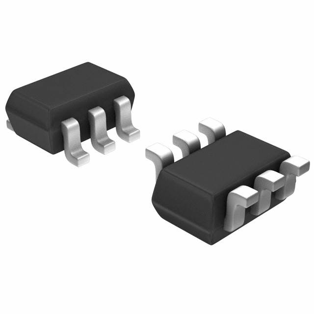
The DG3157E is available in the compact SC-70-6L
package.
• Direct
cross
to
industry
standard
SN74LVC1G3157, NC7SB3157, NLASB3157,
Pl5A3157, and STG3157
• Low switch on-resistance (6 )
• +1.65 V to +5.5 V single supply operation
• Powered-off protection
• Control logic inputs can go over V+ up to 5.5 V
• Low parasitic capacitance, 7 pF at switch off
• Break before make switching
• Latch-up performance exceeds 200 mA per JESD 78
• High ESD rating
- 7000 V human body model (JS-001)
- 1000 V charge device model (JS-002)
• Material categorization: for definitions of compliance
please see www.vishay.com/doc?99912
APPLICATIONS
• Battery powered devices
• Consumer and computing
• Instrumentation
• Medical equipment
• Control and automation
FUNCTIONAL BLOCK DIAGRAM AND PIN CONFIGURATION
SC-70
6-Pin
B1
1
6
S
GND
2
5
V+
B0
3
4
A
Top view
Device marking: H0
TRUTH TABLE
ORDERING INFORMATION
LOGIC INPUT (S)
FUNCTION
0
B0 connected to A
1
B1 connected to A
S18-0421-Rev. C, 23-Apr-18
TEMP. RANGE
-40 °C to +85 °C
PACKAGE
PART NUMBER
SC-70-6
DG3157EDL-T1-GE3
(halogen-free)
Document Number: 76387
1
For technical questions, contact: analogswitchtechsupport@vishay.com
THIS DOCUMENT IS SUBJECT TO CHANGE WITHOUT NOTICE. THE PRODUCTS DESCRIBED HEREIN AND THIS DOCUMENT
ARE SUBJECT TO SPECIFIC DISCLAIMERS, SET FORTH AT www.vishay.com/doc?91000
�DG3157E
www.vishay.com
Vishay Siliconix
ABSOLUTE MAXIMUM RATINGS
PARAMETER
V+, A, B0, B1, S reference to GND
Continuous current (any terminal)
Peak current (pulsed at 1 ms, 10 % duty cycle)
Storage temperature
D suffix
Power dissipation (packages) a
6-pin SC-70 b
ESD / HBM
JS-001
ESD / CDM
JS-002
Latch up
Per JESD78 with 1.5 x Vabs max. clamp
LIMIT
UNIT
-0.3 to 6
± 50
± 200
-65 to +150
250
7000
1000
200
V
mA
°C
mW
V
mA
Notes
a. All leads welded or soldered to PC board
b. Derate 3.1 mW/°C above 70 °C
Stresses beyond those listed under “Absolute Maximum Ratings” may cause permanent damage to the device. These are stress ratings only, and functional operation
of the device at these or any other conditions beyond those indicated in the operational sections of the specifications is not implied. Exposure to absolute maximum
rating conditions for extended periods may affect device reliability.
SPECIFICATIONS
PARAMETER
SYMBOL
TEST CONDITIONS
UNLESS OTHERWISE SPECIFIED
VS = 0.25 V+ or 0.75 V+, V+ = 1.65 V to 1.95 V e
VS = 0.2 V+ or 0.65 V+, V+ = 2.3 V to 5.5 V e
TEMP. a
LIMITS
-40 °C to +85 °C
MIN. b
TYP. c
MAX. b
Full
Full
Full
Full
Full
Full
Full
Full
Full
Full
Full
Full
Full
Room
Room
Room
Room
Room
Room
Room
Room
Room
Full
Room
Full
Room
Full
Full
Full
0.75 V+
0.65 V+
-0.1
-1
-0.1
-1
-0.1
-1
-
8
6
7
10
9
13
12
20
18
2
4
10
58
0.09
0.13
0.15
0.16
-
0.25 V+
0.2 V+
11
9
9
14
12
18
16
26
23
0.1
1
0.1
1
0.1
1
5
5
Full
Room
Full
1.65
-
-
5.5
1
5
UNIT
DC Characteristics
High level input voltage
VSH
Low level input voltage
VSL
On resistance
RON
On resistance flatness
RFLAT
On resistance matching
between channels
RON
V+ = 1.65 V to 1.95 V
V+ = 2.3 V to 5.5 V
V+ = 1.65 V to 1.95 V
V+ = 2.3 V to 5.5 V
VBN = 0 V, IA = 30 mA
VBN = 2.3 V, IA = -30 mA
V+ = 4.5 V
VBN = 4.5 V, IA = -30 mA
VBN = 0 V, IA = 24 mA
V+ = 3 V
VBN = 3 V, IA = -24 mA
VBN = 0 V, IA = 8 mA
V+ = 2.3 V
VBN = 2.3 V, IA = -8 mA
VBN = 0 V, IA = 4 mA
V+ = 1.65 V
VBN = 1.65 V, IA = -4 mA
V+ = 4.5 V, IA = -30 mA
V+ = 3 V, IA = -24 mA
0 < VBN < V+
V+ = 2.3 V, IA = -8 mA
V+ = 1.65 V, IA = -4 mA
V+ = 4.5 V, VBN = 3.15 V, IA = -30 mA
V+ = 3 V, VBN = 2.1 V, IA = -24 mA
V+ = 2.3 V, VBN = 1.6 V, IA = -8 mA
V+ = 1.65 V, VBN = 1.15 V, IA = -4 mA
IS
V+ = 5.5 V, VS = 5.5 V
Off stage switch leakage
IBN(off)
V+ = 5.5 V, VA = 1 V / 4.5 V, VB = 4.5 V / 1 V
On state switch leakage
IBN(on)
V+ = 5.5 V, VA = VB = 1 V or 4.5 V
Power down leakage
IPD
V+ = 0 V, VA = 5 V, B0, B1 open, VS = GND
V+ = 0 V, VB0, VB1 = 5 V, A open, VS = GND
Power Supply
Power supply range
V+
Quiescent supply current
I+
Input leakage current
S18-0421-Rev. C, 23-Apr-18
V+ = 5.5 V, VS = V+ or GND
V
μA
V
μA
Document Number: 76387
2
For technical questions, contact: analogswitchtechsupport@vishay.com
THIS DOCUMENT IS SUBJECT TO CHANGE WITHOUT NOTICE. THE PRODUCTS DESCRIBED HEREIN AND THIS DOCUMENT
ARE SUBJECT TO SPECIFIC DISCLAIMERS, SET FORTH AT www.vishay.com/doc?91000
�DG3157E
www.vishay.com
Vishay Siliconix
SPECIFICATIONS
PARAMETER
SYMBOL
TEST CONDITIONS
UNLESS OTHERWISE SPECIFIED
VS = 0.25 V+ or 0.75 V+, V+ = 1.65 V to 1.95 V e
VS = 0.2 V+ or 0.65 V+, V+ = 2.3 V to 5.5 V e
LIMITS
-40 °C to +85 °C
TEMP. a
UNIT
MIN. b
TYP. c
MAX. b
-
AC Electrical Characteristics e
Prop delay time f
tPHL/tPLH
VA = 0 V,
see Fig. 3
V+ = 1.65 V to 1.95 V
Full
-
4
V+ = 2.3 V to 2.7 V
Full
-
3
-
V+ = 3 V to 3.6 V
Full
-
2
-
V+ = 4.5 V to 5.5 V
V+ = 1.65 V to 1.95 V
Output enable time f
tPZL/tPZH
VLOAD = 2 x V+
for tPZL,
VLOAD = 0 V
for tPZH,
see Fig. 4
V+ = 2.3 V to 2.7 V
V+ = 3 V to 3.6 V
V+ = 4.5 V to 5.5 V
V+ = 1.65 V to 1.95 V
Output disable time f
tPLZ/tPHZ
VLOAD = 2 x V+
for tPLZ,
VLOAD = 0 V
for tPHZ,
see Fig. 4
V+ = 2.3 V to 2.7 V
V+ = 3 V to 3.6 V
V+ = 4.5 V to 5.5 V
Break-before-make time d
tBBM
Charge injection d
Q
Full
-
2
-
Room
-
32
-
Full
-
34
-
Room
-
22
-
Full
-
23
-
Room
-
19
-
Full
-
20
-
Room
-
16
-
Full
-
16
-
Room
-
22
-
Full
-
23
-
Room
-
18
-
Full
-
19
-
Room
-
16
-
Full
-
16
-
Room
-
13
-
Full
-
14
V+ = 1.65 V to 1.95 V
Full
0.5
-
-
V+ = 2.3 V to 2.7 V
Full
0.5
-
-
V+ = 3 V to 3.65 V
Full
0.5
-
-
V+ = 4.5 V to 5.5 V
Full
0.5
-
-
V+ = 5 V
Room
-
1.3
-
V+ = 3.3 V
Room
-
0.5
-
CL = 0.1 nF,
VGEN = 0 V
RGEN = 0
ns
pC
Analog Switch Characteristics
Off isolation d
OIRR
Crosstalk d
XTALK
-3 dB bandwidth d
RL = 50 , f = 10 MHz
BW
RL = 50
CIN
V+ = 0 V
Room
-
-61
-
Room
-
-61
-
Room
-
580
-
dB
MHz
Capacitance
Control pin capacitance d
B port off capacitance d
A port capacitance when
switch enable d
CIO-B
CIO-A(on)
V+ = 5 V
Room
-
6
-
Room
-
7
-
Room
-
12
-
pF
Notes
a. Room = 25 °C, full = as determined by the operating suffix
b. The algebraic convention whereby the most negative value is a minimum and the most positive a maximum, is used in this datasheet
c. Typical values are for design aid only, not guaranteed nor subject to production testing
d. Guarantee by design, nor subjected to production test
e. VS = input voltage to perform proper function
f. Guaranteed by design and not production tested. The bus switch propagation delay is a function of the RC time constant contributed by the
on-resistance and the specified load capacitance with an ideal voltage source (zero output impedance) driving the switch
S18-0421-Rev. C, 23-Apr-18
Document Number: 76387
3
For technical questions, contact: analogswitchtechsupport@vishay.com
THIS DOCUMENT IS SUBJECT TO CHANGE WITHOUT NOTICE. THE PRODUCTS DESCRIBED HEREIN AND THIS DOCUMENT
ARE SUBJECT TO SPECIFIC DISCLAIMERS, SET FORTH AT www.vishay.com/doc?91000
�DG3157E
www.vishay.com
Vishay Siliconix
LOGIC DIAGRAM POSITIVE LOGIC
B1
S
A
B0
Fig. 1
TYPICAL CHARACTERISTICS (25 °C, unless otherwise noted)
10000
V+ = +1.65 V, IS = 4 mA
2nd line
RON - On-Resistance (Ω)
70
60
1000
1st line
2nd line
50
40
V+ = +2.3 V, IS = 8 mA
30
100
V+ = +3.0 V, IS = 24 mA
20
V+ = +4.5 V, IS = 30 mA
10
0
10
IA(PD) Power Down Leakage Current (nA)
0
1
2
3
4
5
IA(PD) Power Down Leakage Current (nA)
Axis Title
80
2.5
V+ = VS = GND,
VA= +3 V
2
1.5
1
0.5
0
-40
-20
0
20
40
60
80
100
VA - Analog Voltage (V)
2nd line
Temperature (°C)
2nd line
RON vs. VA vs. V+
Power Down Leakage Current vs. Temperature
8
V+ = VS = GND
7
6
5
4
85 °C
3
2
-40 °C
1
25 °C
0
0
2
4
6
VA (V)
2nd line
Power Down Leakage Current vs. VA
S18-0421-Rev. C, 23-Apr-18
Document Number: 76387
4
For technical questions, contact: analogswitchtechsupport@vishay.com
THIS DOCUMENT IS SUBJECT TO CHANGE WITHOUT NOTICE. THE PRODUCTS DESCRIBED HEREIN AND THIS DOCUMENT
ARE SUBJECT TO SPECIFIC DISCLAIMERS, SET FORTH AT www.vishay.com/doc?91000
�DG3157E
www.vishay.com
Vishay Siliconix
AC LOADING AND WAVEFORMS
V LD
RL
500
From output
under test
SW
Open
GND
RL
500
CL
50 pF
TEST
SW
tPLH/tPHL
Open
tPLZ/tPZL
V LD
tPHZ/tPZH
GND
Load circuit
Fig. 2 - AC Test Circuit
tr = 2.5 ns
tf = 2.5 ns
V+
90 %
Switch
input
tf = 2.5 ns
90 %
1.5 V
90 %
Logic
input
1.5 V
10 %
tr = 2.5 ns
1.5 V
1.5 V
10 %
10 %
10 %
GND
GND
tw
tPLZ
tPZL
tPHL
tPLH
V OH
1.5 V
V OL + 0.3 V
Waveform 1
SW at V LD
1.5 V
VLD
2
1.5 V
Output
Output
V+
90 %
V OL
tPZH
tPHZ
V OH
V OL
V OH 0.3 V
Output
waveform 2
SW at GND
Propagation delay times
Fig. 3 - AC Waveforms
1.5 V
0V
Enable and disable time-low- and high-level enabling
Fig. 4 - AC Waveforms
Notes
• CL includes probe and jig capacitance
• Waveform 1 is for an output with internal conditions such that the output is low except when disabled by the output control
• Waveform 2 is for an output with internal conditions such that the output is high except when disabled by the output control.
• All input pulses are supplied by generators having the following characteristics: PRR 10 MHz, ZO = 50
• The outputs are measured one at a time with one transition per measurement
• tPLZ and tPHZ are the same as tdis
• tPZL and tPZH are the same as tdis
• tPLH and tPHL are the same as tdis
• VLD = 2 V+
S18-0421-Rev. C, 23-Apr-18
Document Number: 76387
5
For technical questions, contact: analogswitchtechsupport@vishay.com
THIS DOCUMENT IS SUBJECT TO CHANGE WITHOUT NOTICE. THE PRODUCTS DESCRIBED HEREIN AND THIS DOCUMENT
ARE SUBJECT TO SPECIFIC DISCLAIMERS, SET FORTH AT www.vishay.com/doc?91000
�DG3157E
www.vishay.com
Vishay Siliconix
TEST CIRCUITS
V+
B1
B0
VSH
Logic
Input
V+
A
B1
tr < 5 ns
tf < 5 ns
VSL
VO
B0
RL
50 Ω
S
CL
35 pF
VB = VB
0
1
VO
GND
90 %
Switch
0V
Output
tD
tD
CL (includes fixture and stray capacitance)
Fig. 5 - Break-Before-Make Interval
V+
V+
Rgen
OUT
VA
A
BX
VOUT
+
S
Vgen
VS
CL = 1 nF
VIN = 0 – V+
On
On
Off
GND
Q=
OUT
x CL
IN depends on switch configuration: input polarity
determined by sense of switch.
Fig. 6 - Charge Injection
V+
V+
10 nF
10 nF
V+
V+
BX
S
A
0 V, 2.4 V
Meter
COM
A
S
0 V, 2.4 V
RL
BX
GND
GND
Analyzer
HP4192A
Impedance
Analyzer
or Equivalent
f = 1 MHz
VA
Off Isolation = 20 log V
Bx
Fig. 7 - Off-Isolation
Fig. 8 - Channel Off/On Capacitance
Vishay Siliconix maintains worldwide manufacturing capability. Products may be manufactured at one of several qualified locations. Reliability data for Silicon
Technology and Package Reliability represent a composite of all qualified locations. For related documents such as package / tape drawings, part marking, and
reliability data, see www.vishay.com/ppg?76387.
S18-0421-Rev. C, 23-Apr-18
Document Number: 76387
6
For technical questions, contact: analogswitchtechsupport@vishay.com
THIS DOCUMENT IS SUBJECT TO CHANGE WITHOUT NOTICE. THE PRODUCTS DESCRIBED HEREIN AND THIS DOCUMENT
ARE SUBJECT TO SPECIFIC DISCLAIMERS, SET FORTH AT www.vishay.com/doc?91000
�Legal Disclaimer Notice
www.vishay.com
Vishay
Disclaimer
ALL PRODUCT, PRODUCT SPECIFICATIONS AND DATA ARE SUBJECT TO CHANGE WITHOUT NOTICE TO IMPROVE
RELIABILITY, FUNCTION OR DESIGN OR OTHERWISE.
Vishay Intertechnology, Inc., its affiliates, agents, and employees, and all persons acting on its or their behalf (collectively,
“Vishay”), disclaim any and all liability for any errors, inaccuracies or incompleteness contained in any datasheet or in any other
disclosure relating to any product.
Vishay makes no warranty, representation or guarantee regarding the suitability of the products for any particular purpose or
the continuing production of any product. To the maximum extent permitted by applicable law, Vishay disclaims (i) any and all
liability arising out of the application or use of any product, (ii) any and all liability, including without limitation special,
consequential or incidental damages, and (iii) any and all implied warranties, including warranties of fitness for particular
purpose, non-infringement and merchantability.
Statements regarding the suitability of products for certain types of applications are based on Vishay’s knowledge of
typical requirements that are often placed on Vishay products in generic applications. Such statements are not binding
statements about the suitability of products for a particular application. It is the customer’s responsibility to validate that a
particular product with the properties described in the product specification is suitable for use in a particular application.
Parameters provided in datasheets and / or specifications may vary in different applications and performance may vary over
time. All operating parameters, including typical parameters, must be validated for each customer application by the customer’s
technical experts. Product specifications do not expand or otherwise modify Vishay’s terms and conditions of purchase,
including but not limited to the warranty expressed therein.
Except as expressly indicated in writing, Vishay products are not designed for use in medical, life-saving, or life-sustaining
applications or for any other application in which the failure of the Vishay product could result in personal injury or death.
Customers using or selling Vishay products not expressly indicated for use in such applications do so at their own risk.
Please contact authorized Vishay personnel to obtain written terms and conditions regarding products designed for
such applications.
No license, express or implied, by estoppel or otherwise, to any intellectual property rights is granted by this document
or by any conduct of Vishay. Product names and markings noted herein may be trademarks of their respective owners.
© 2017 VISHAY INTERTECHNOLOGY, INC. ALL RIGHTS RESERVED
Revision: 08-Feb-17
1
Document Number: 91000
�