Product is End of Life
DG3516, DG3517
Vishay Siliconix
300 MHz, 2.5 Ω, Dual SPDT Analog Switches
DESCRIPTION
FEATURES
The DG3516, DG3517 are dual SPDT analog switches which
operate from 1.8 V to 5.5 V single rail power supply. They are
design for audio, video, and USB switching applications.
The devices have 2.5 Ω on-resistance and 300 MHz 3dB
bandwidth. 0.2 Ω on-resistance matching and 1 Ω flatness
make the device high linearity. The devices are 1.6 V logic
compatible within the full operation voltage range.
These switches are built on a sub-micron high density
process that brings low power consumption and low voltage
performance.
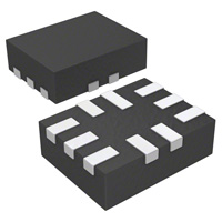
The switches are packaged in MICRO FOOT chip scale
package of 4 mm x 3 mm bump array.
As a committed partner to the community and environment,
Vishay Siliconix manufactures this product with the
lead (Pb)-free device terminations. For MICRO FOOT analog
switch products manufactured with tin/silver/copper
(SnAgCu) device termination, the lead (Pb)-free “-E1” suffix
is being used as a designator.
• Halogen-free according to IEC 61249-2-21
Definition
• 1.8 V to 5.5 V operation
• 2.5 Ω at 2.7 V RON
• 300 MHz - 3 dB bandwidth
• ESD method 3015.7 > 2 kV
• Latch-up current 200 mA (JESD 78)
• 1.6 V logic compatible
• Compliant to RoHS Directive 2002/95/EC
BENEFITS
•
•
•
•
•
Space Saving MICRO FOOT® Package
High Linearity
Low Power Consumption
High Bandwidth
Full Rail Signal Swing Range
APPLICATIONS
•
•
•
•
•
•
Cellular Phones
MP3
Media Players
Modems
Hard Drives
PCMCIA
FUNCTIONAL BLOCK DIAGRAM AND PIN CONFIGURATION
DG3516/DG3517
MICRO FOOT 10-Bump
1
2
3
NC2
IN2
4
V+
A
COM2
NO2
IN1
B
NO1
DG3516
GND
Top View
COM1
NC1
NO2
COM2
NC2
C
NC1
IN1
1
2
COM1
V+
TRUTH TABLE
Logic
NC1 and NC2
NO1 and NO2
0
ON
OFF
1
OFF
ON
NO1
IN2
GND
Device Marking
3
4
ORDERING INFORMATION
A
NO2
IN2
COM2
NC2
A1 Locator
XXX
3516
B
GND
C
NO1
DG3517
Top View
IN1
COM1
V+
Temp. Range
Package
Part Number
- 40 °C to 85 °C
MICRO FOOT: 10 Bump
(4 x 3, 0.5 mm Pitch,
238 µm Bump Height)
DG3516DB-T5-E1
DG3517DB-T5-E1
NC1
3516 = Example Base Part Number
xxx = Data/Lot Traceabiliity Code
Document Number: 73404
S11-1185-Rev. D, 13-Jun-11
www.vishay.com
1
This document is subject to change without notice.
THE PRODUCTS DESCRIBED HEREIN AND THIS DOCUMENT ARE SUBJECT TO SPECIFIC DISCLAIMERS, SET FORTH AT www.vishay.com/doc?91000
�Product is End of Life
DG3516, DG3517
Vishay Siliconix
ABSOLUTE MAXIMUM RATINGS
Parameter
Limit
Reference V+ to GND
Unit
- 0.3 to + 6
IN, COM, NC, NOa
V
- 0.3 to (V+ + 0.3)
Continuous Current (NO, NC, COM)
± 100
Peak Current (Pulsed at 1 ms, 10 % duty cycle)
± 200
Storage Temperature
(D Suffix)
b
Package Solder Reflow Conditions
- 65 to 150
°C
IR/Convection
250
>2
kV
MICRO FOOT: 10 Bump (4 mm x 3 mm)d
457
mW
ESD per Method 3015.7
Power Dissipation (Packages)c
mA
Notes:
a. Signals on NC, NO, or COM or IN exceeding V+ will be clamped by internal diodes. Limit forward diode current to maximum current ratings.
b. Refer to IPC/JEDEC (J-STD-020B).
c. All bumps welded or soldered to PC board.
d. Derate 5.7 mW/°C above 70 °C.
Stresses beyond those listed under “Absolute Maximum Ratings” may cause permanent damage to the device. These are stress ratings only, and functional operation
of the device at these or any other conditions beyond those indicated in the operational sections of the specifications is not implied. Exposure to absolute maximum
rating conditions for extended periods may affect device reliability.
SPECIFICATIONS (V+ = 3 V)
Limits
- 40 °C to 85 °C
Test Conditions
Otherwise Unless Specified
Parameter
Symbol
V+ = 2.7 V to 3.6 V, VIN = 0.5 V or 1.4 Ve
Temp.a
Min.b
Full
0
Typ.c
Max.b
Unit
V+
V
Analog Switch
Analog Signal Ranged
On-Resistanced
RON Flatnessd
On-Resistance
Match Between Channelsd
Switch Off Leakage Current
VNO, VNC,
VCOM
RON
RON
Flatness
ΔRDS(on)
INO(off)
INC(off)
ICOM(off)
Channel-On Leakage Current
ICOM(on)
V+ = 2.7 V
INO, INC = 10 mA
VCOM = 1.5 V
Room
Full
2.5
3.5
3.8
VCOM = 1, 1.5, 2 V
Room
0.52
1
VCOM = 1.5 V
Room
V+ = 3.3 V,
VNO, VNC = 0.3 V/3 V, VCOM = 3 V/0.3 V
V+ = 3.3 V, VNO, VNC = VCOM = 0.3 V/3 V
Ω
0.25
Room
Full
-2
- 20
2
20
Room
Full
-2
- 20
2
20
Room
Full
-2
- 20
2
20
1.4
nA
Digital Control
Input High Voltaged
VINH
Full
Input Low Voltage
VINL
Full
Input Capacitance
Input Current
www.vishay.com
2
Cin
IINL or IINH
0.5
Full
VIN = 0 V or V+
Full
5
1
V
pF
1
µA
Document Number: 73404
S11-1185-Rev. D, 13-Jun-11
This document is subject to change without notice.
THE PRODUCTS DESCRIBED HEREIN AND THIS DOCUMENT ARE SUBJECT TO SPECIFIC DISCLAIMERS, SET FORTH AT www.vishay.com/doc?91000
�Product is End of Life
DG3516, DG3517
Vishay Siliconix
SPECIFICATIONS (V+ = 3 V)
Limits
- 40 °C to 85 °C
Test Conditions
Otherwise Unless Specified
Parameter
Symbol
V+ = 2.7 V to 3.6 V, VIN = 0.5 V or 1.4 Ve
Temp.a
Min.b
Typ.c
Max.b
Room
Full
21
51
52
Room
Full
15
45
46
Unit
Dynamic Characteristics
Turn-On Time
tON
Turn-Off Time
tOFF
td
Break-Before-Make Time
Charge Injection
V+ = 2.7 V, VNO or VNC = 1.5 V
RL = 300 Ω, CL = 35 pF
d
QINJ
Off-Isolationd
Full
Room
1
f = 1 MHz
Room
- 74
f = 10 MHz
Room
- 54
f = 1 MHz
Room
- 76
f = 10 MHz
RL = 50 Ω, CL = 5 pF
Crosstalkd
XTALK
NO, NC Off Capacitanced
d
Channel-On Capacitance
1
CL = 1 nF, VGEN = 2 V, RGEN = 0 Ω
OIRR
Room
- 56
CNO(off)
Room
12
CNC(off)
Room
12
Room
40
Room
40
CNO(on)
VIN = 0 or V+, f = 1 MHz
CNC(on)
ns
pC
dB
pF
Power Supply
Power Supply Current
Document Number: 73404
S11-1185-Rev. D, 13-Jun-11
I+
VIN = 0 V or V+
Room
Full
1
1
µA
www.vishay.com
3
This document is subject to change without notice.
THE PRODUCTS DESCRIBED HEREIN AND THIS DOCUMENT ARE SUBJECT TO SPECIFIC DISCLAIMERS, SET FORTH AT www.vishay.com/doc?91000
�Product is End of Life
DG3516, DG3517
Vishay Siliconix
SPECIFICATIONS (V+ = 5 V)
Limits
- 40 °C to 85 °C
Test Conditions
Otherwise Unless Specified
Parameter
Symbol
V+ = 4.2 V to 5.5 V, VIN = 0.8 V or 2 Ve
Temp.a
Min.b
Full
0
Typ.c
Max.b
Unit
V+
V
Analog Switch
VNO, VNC,
VCOM
Analog Signal Ranged
On-Resistanced
RON
RON Flatnessd
RON
Flatness
On-Resistance
ΔRDS(on)
Match Between Channelsd
Switch Off Leakage Current
INO(off)
INC(off)
ICOM(off)
Channel-On Leakage Current
ICOM(on)
V+ = 4.2 V
INO, INC = 10 mA
VCOM = 3.5 V
Room
Full
2.2
2.9
3.1
VCOM = 1, 2, 3.5 V
Room
0.53
1
VCOM = 3.5 V
Room
V+ = 5.5 V,
VNO, VNC = 1 V/4.5 V, VCOM = 4.5 V/1 V
V+ = 5.5 V, VNO, VNC = VCOM = 1 V/4.5 V
Ω
0.25
Room
Full
-2
- 20
2
20
Room
Full
-2
- 20
2
20
Room
Full
-2
- 20
2
20
2
nA
Digital Control
Input High Voltaged
VINH
Full
Input Low Voltage
VINL
Full
Input Capacitance
Cin
Full
IINL or IINH
Input Current
VIN = 0 or V+
Full
0.8
5
1
V
pF
1
µA
Dynamic Characteristics
Turn-On Time
tON
Turn-Off Time
tOFF
td
Break-Before-Make Time
Charge Injection
V+ = 4.2 V, VNO or VNC = 3 V
RL = 300 Ω, CL = 35 pF
d
QINJ
Off-Isolationd
RL = 50 Ω, CL = 5 pF
XTALK
NO, NC Off Capacitanced
Channel-On Capacitance
d
15
45
46
Room
Full
12
42
43
Full
CL = 1 nF, VGEN = 2 V, RGEN = 0 Ω
OIRR
Crosstalkd
Room
Full
1
Room
1
f = 1 MHz
Room
- 74
f = 10 MHz
Room
- 54
f = 1 MHz
Room
- 78
f = 10 MHz
Room
- 56
CNO(off)
Room
12
CNC(off)
Room
12
Room
40
Room
40
CNO(on)
VIN = 0 or V+, f = 1 MHz
CNC(on)
ns
pC
dB
pF
Power Supply
Power Supply Current
I+
VIN = 0 V or V+
Room
Full
1
1
µA
Notes:
a. Room = 25 °C, Full = as determined by the operating suffix.
b. Typical values are for design aid only, not guaranteed nor subject to production testing.
c. The algebraic convention whereby the most negative value is a minimum and the most positive a maximum, is used in this datasheet.
d. Guarantee by design, nor subjected to production test.
e. VIN = input voltage to perform proper function.
f. Guaranteed by 5 V testing, not production tested.
www.vishay.com
4
Document Number: 73404
S11-1185-Rev. D, 13-Jun-11
This document is subject to change without notice.
THE PRODUCTS DESCRIBED HEREIN AND THIS DOCUMENT ARE SUBJECT TO SPECIFIC DISCLAIMERS, SET FORTH AT www.vishay.com/doc?91000
�Product is End of Life
DG3516, DG3517
Vishay Siliconix
TYPICAL CHARACTERISTICS (25 °C, unless otherwise noted)
8
T = 25 °C
IS = 10 mA
R ON - On-Resistance (Ω)
7
V+ = 1.8 V
V+ = 2.0 V
V+ = 2.7 V
V+ = 3.0 V
V+ = 3.6 V
V+ = 4.2 V
V+ = 5.0 V
V+ = 5.5 V
6
5
4
3
2
1
0
0
1
2
3
5
4
VCOM - Analog Voltage (V)
RON vs. VCOM and Single Supply Voltage
5
4.0
V+ = 2.7 V
IS = 10 mA
V+ = 4.2 V
IS = 10 mA
3.5
R ON - On-Resistance (Ω)
R ON - On-Resistance (Ω)
4
3
2
85 °C
25 °C
- 40 °C
1
3.0
2.5
2.0
1.5
85 °C
25 °C
- 40 °C
1.0
0.5
0
0.0
0.0
0.5
1.0
1.5
2.0
2.5
0
3.0
1
2
3
VCOM - Analog Voltage (V)
VCOM - Analog Voltage (V)
RON vs. Analog Voltage and Temperature
100 mA
10 mA
V+ = 3.0 V
VIN = 0 V
I+ - Supply Current (A)
I+ - Supply Current (nA)
5
RON vs. Analog Voltage and Temperature
100 000
10 000
4
1000
100
V+ = 3.0 V
1 mA
100 µA
10 µA
1 µA
100 nA
10 nA
10
- 60
- 40
- 20
0
20
40
60
Temperature (°C)
Supply Current vs. Temperature
Document Number: 73404
S11-1185-Rev. D, 13-Jun-11
80
100
1 nA
10
100
1K
10K
100K
1M
Input Switching Frequency (Hz)
10M
Supply Current vs. Input Switching Frequency
www.vishay.com
5
This document is subject to change without notice.
THE PRODUCTS DESCRIBED HEREIN AND THIS DOCUMENT ARE SUBJECT TO SPECIFIC DISCLAIMERS, SET FORTH AT www.vishay.com/doc?91000
�Product is End of Life
DG3516, DG3517
Vishay Siliconix
TYPICAL CHARACTERISTICS (25 °C, unless otherwise noted)
10 000
800
V+ = 3.6 V
V+ = 3.0 V
600
400
Leakage Current (pA)
Leakage Current (pA)
1000
ICOM(off)
ICOM(on)
100
INO(off), INC(off)
200
ICOM(on)
INO(off), INC(off)
0
- 200
ICOM(off)
- 400
10
- 600
1
- 60
- 800
- 40
- 20
0
20
40
Temperature (°C)
60
80
100
0.0
0.6
Leakage Current vs. Temperature
2.4
3.0
3.6
10
tON V+ = 2.7 V
Loss
- 10
20
Loss, OIRR, X TALK (dB)
t ON / t OFF - Switching Time (ns)
1.8
Leakage vs. Analog Voltage
25
tON V+ = 4.2 V
15
tOFF V+ = 4.2 V
10
tOFF V+ = 2.7 V
5
XTALK
OIRR
- 30
- 50
V+ = 3.0 V
RL
- 70
0
- 60
- 40
- 20
0
20
40
Temperature (°C)
60
80
100
- 90
100 K
1M
10M
100M
1G
Frequency (Hz)
Switching Time vs. Temperature
Insertion Loss, Off-Isolation
Crosstalk vs. Frequency
10
2.00
8
1.75
6
1.50
Q - Charge Injection (pC)
VT - Switching Threshold (V)
1.2
VCOM, V NO, V NC - Analog Voltage (V)
1.25
1.00
0.75
0.50
V+ = 3.0 V
4
V+ = 2.0 V
2
V+ = 5.0 V
0
-2
-4
-6
0.25
-8
0.00
- 10
0
1
2
3
4
V+ - Supply Voltage (V)
5
Switching Threshold vs. Supply Voltage
www.vishay.com
6
6
0
1
2
3
VCOM - Analog Voltage (V)
4
5
Charge Injection vs. Analog Voltage
Document Number: 73404
S11-1185-Rev. D, 13-Jun-11
This document is subject to change without notice.
THE PRODUCTS DESCRIBED HEREIN AND THIS DOCUMENT ARE SUBJECT TO SPECIFIC DISCLAIMERS, SET FORTH AT www.vishay.com/doc?91000
�Product is End of Life
DG3516, DG3517
Vishay Siliconix
TEST CIRCUITS
V+
VINH
Logic
Input
50 %
V+
NO or NC
Switch
Input
VINL
Switch Output
COM
tr < 5 ns
tf < 5 ns
VOUT
0.9 x V OUT
IN
Logic
Input
RL
300 Ω
GND
Switch
Output
CL
35 pF
0V
tOFF
tON
0V
Logic “1” = Switch On
Logic input waveforms inverted for switches that have
the opposite logic sense.
CL (includes fixture and stray capacitance)
VOUT = VCOM
(
RL
R L + R ON
)
Figure 1. Switching Time
V+
Logic
Input
V+
COM
NO
VNO
VO
VINH
tr < 5 ns
tf < 5 ns
VINL
NC
VNC
RL
300 Ω
IN
CL
35 pF
GND
VNC = V NO
VO
90 %
Switch
0V
Output
tD
tD
CL (includes fixture and stray capacitance)
Figure 2. Break-Before-Make Interval
V+
ΔV OUT
VOUT
Rgen
V+
COM
NC or NO
VOUT
+
IN
IN
On
Off
On
CL = 1 nF
VIN = 0 - V+
Q = ΔVOUT x CL
GND
IN depends on switch configuration: input polarity
determined by sense of switch.
Figure 3. Charge Injection
Document Number: 73404
S11-1185-Rev. D, 13-Jun-11
www.vishay.com
7
This document is subject to change without notice.
THE PRODUCTS DESCRIBED HEREIN AND THIS DOCUMENT ARE SUBJECT TO SPECIFIC DISCLAIMERS, SET FORTH AT www.vishay.com/doc?91000
�Product is End of Life
DG3516, DG3517
Vishay Siliconix
TEST CIRCUITS
V+
10 nF
V+
NC or NO
IN
COM
COM
RL
Analyzer
0 V, 2.4 V
GND
VCOM
Off Isolation = 20 log V
NO/ NC
Figure 4. Off-Isolation
V+
10 nF
V+
COM
Meter
IN
0 V, 2.4 V
NC or NO
GND
HP4192A
Impedance
Analyzer
or Equivalent
f = 1 MHz
Figure 5. Channel Off/On Capacitance
www.vishay.com
8
Document Number: 73404
S11-1185-Rev. D, 13-Jun-11
This document is subject to change without notice.
THE PRODUCTS DESCRIBED HEREIN AND THIS DOCUMENT ARE SUBJECT TO SPECIFIC DISCLAIMERS, SET FORTH AT www.vishay.com/doc?91000
�Product is End of Life
DG3516, DG3517
Vishay Siliconix
PACKAGE OUTLINE
MICRO FOOT: 10 BUMP (4 x 3 0.5 mm PITCH, 0.238 mm BUMP HEIGHT)
10 X Ø 0.150 ∼ 0.229
Note b
Solder Mask Ø ∼ Pad Diameter + 0.1
Silicon
0.5
A2
A
A1
Bump
Note a
0.5
4
Recommended Land Pattern
3
2
1
b Diameter
A
e
Index-Bump A1
Note c
B
E
e
XXX
3516
C
S
S
e
e
e
Top Side (Die Back)
D
Notes (Unless Otherwise Specified):
a. Bump is Lead (Pb)-free Sn/Ag/Cu.
b. Non-solder mask defined copper landing pad.
c. Laser Mark on silicon die back; back-lapped, no coating. Shown is not actual marking; sample only.
Dim.
Millimetersa
Inches
Min.
Max.
Min.
Max.
A
0.688
0.753
0.0271
0.0296
A1
0.218
0.258
0.0086
0.0102
A2
0.470
0.495
0.0185
0.0195
b
0.306
0.346
0.0120
0.0136
D
1.980
2.020
0.0780
0.0795
E
1.480
1.520
0.0583
e
S
0.5 BASIC
0.230
0.0598
0.0197 BASIC
0.270
0.0091
0.0106
Notes:
a. Use millimeters as the primary measurement.
Vishay Siliconix maintains worldwide manufacturing capability. Products may be manufactured at one of several qualified locations. Reliability data for Silicon
Technology and Package Reliability represent a composite of all qualified locations. For related documents such as package/tape drawings, part marking, and
reliability data, see www.vishay.com/ppg?73404.
Document Number: 73404
S11-1185-Rev. D, 13-Jun-11
www.vishay.com
9
This document is subject to change without notice.
THE PRODUCTS DESCRIBED HEREIN AND THIS DOCUMENT ARE SUBJECT TO SPECIFIC DISCLAIMERS, SET FORTH AT www.vishay.com/doc?91000
�Package Information
Vishay Siliconix
MICRO FOOT: 10-BUMP (4 mm x 3 mm, 0.5 mm PITCH, 0.238 mm BUMP HEIGHT)
10 X Ø 0.150 ~ 0.229
Note b
Solder Mask Ø ~ Pad Diameter + 0.1
Silicon
0.5
A2
A
A1
Bump
Note a
0.5
3
4
Recommended Land Pattern
2
1
b Diameter
A
e
Index-Bump A1
Note c
B
E
e
XXX
3535
C
S
S
e
e
e
Top Side (Die Back)
D
Notes
(unless otherwise specified)
a. Bump is lead (Pb)-free Sn/Ag/Cu.
b. Non-solder mask defined copper landing pad.
c. Laser mark on silicon die back; back-lapped, no coating. Shown is not actual marking; sample only.
DIM.
MILLIMETERSa
INCHES
MIN.
MAX.
MIN.
MAX.
A
0.688
0.753
0.0271
0.0296
A1
0.218
0.258
0.0086
0.0102
A2
0.470
0.495
0.0185
0.0195
0.0136
b
0.306
0.346
0.0120
D
1.980
2.020
0.0780
0.0795
E
1.480
1.520
0.0583
0.0598
e
S
0.5 BASIC
0.230
0.0197 BASIC
0.270
0.0091
0.0106
Note
a. Use millimeters as the primary measurement.
ECN: S11-1065-Rev. A, 13-Jun-11
DWG: 6001
Document Number: 63272
Revision:13-Jun-11
www.vishay.com
1
This document is subject to change without notice.
THE PRODUCTS DESCRIBED HEREIN AND THIS DOCUMENT ARE SUBJECT TO SPECIFIC DISCLAIMERS, SET FORTH AT www.vishay.com/doc?91000
�Legal Disclaimer Notice
www.vishay.com
Vishay
Disclaimer
ALL PRODUCT, PRODUCT SPECIFICATIONS AND DATA ARE SUBJECT TO CHANGE WITHOUT NOTICE TO IMPROVE
RELIABILITY, FUNCTION OR DESIGN OR OTHERWISE.
Vishay Intertechnology, Inc., its affiliates, agents, and employees, and all persons acting on its or their behalf (collectively,
“Vishay”), disclaim any and all liability for any errors, inaccuracies or incompleteness contained in any datasheet or in any other
disclosure relating to any product.
Vishay makes no warranty, representation or guarantee regarding the suitability of the products for any particular purpose or
the continuing production of any product. To the maximum extent permitted by applicable law, Vishay disclaims (i) any and all
liability arising out of the application or use of any product, (ii) any and all liability, including without limitation special,
consequential or incidental damages, and (iii) any and all implied warranties, including warranties of fitness for particular
purpose, non-infringement and merchantability.
Statements regarding the suitability of products for certain types of applications are based on Vishay's knowledge of typical
requirements that are often placed on Vishay products in generic applications. Such statements are not binding statements
about the suitability of products for a particular application. It is the customer's responsibility to validate that a particular product
with the properties described in the product specification is suitable for use in a particular application. Parameters provided in
datasheets and / or specifications may vary in different applications and performance may vary over time. All operating
parameters, including typical parameters, must be validated for each customer application by the customer's technical experts.
Product specifications do not expand or otherwise modify Vishay's terms and conditions of purchase, including but not limited
to the warranty expressed therein.
Hyperlinks included in this datasheet may direct users to third-party websites. These links are provided as a convenience and
for informational purposes only. Inclusion of these hyperlinks does not constitute an endorsement or an approval by Vishay of
any of the products, services or opinions of the corporation, organization or individual associated with the third-party website.
Vishay disclaims any and all liability and bears no responsibility for the accuracy, legality or content of the third-party website
or for that of subsequent links.
Except as expressly indicated in writing, Vishay products are not designed for use in medical, life-saving, or life-sustaining
applications or for any other application in which the failure of the Vishay product could result in personal injury or death.
Customers using or selling Vishay products not expressly indicated for use in such applications do so at their own risk. Please
contact authorized Vishay personnel to obtain written terms and conditions regarding products designed for such applications.
No license, express or implied, by estoppel or otherwise, to any intellectual property rights is granted by this document or by
any conduct of Vishay. Product names and markings noted herein may be trademarks of their respective owners.
© 2022 VISHAY INTERTECHNOLOGY, INC. ALL RIGHTS RESERVED
Revision: 01-Jan-2022
1
Document Number: 91000
�


 工商网监
湘ICP备2023018690号
工商网监
湘ICP备2023018690号
