DG611A, DG612A, DG613A
Vishay Siliconix
1 pC Charge Injection, 100 pA Leakage, Quad SPST Switches
DESCRIPTION
FEATURES
The DG611A, DG612A and DG613A contain four
independently selectable SPST switches. They offer
improved performance over the industry standard DG611
series. The DG611A and DG612A have all switches normally
closed and normally open respectively, while the DG613A
has 2 normally open and 2 normally closed switches.
They are designed to operate from a 2.7 V to 12 V single
supply or from ± 2.7 V to ± 5 V dual supplies and are fully
specified at + 3 V, + 5 V and ± 5 V. All control logic inputs have
guaranteed 2 V logic high limits when operating from + 5 V or
± 5 V supplies and 1.4 V when operating from a + 3 V supply.
The DG611A, DG612A and DG613A switches conduct
equally well in both directions and offer rail to rail analog
signal handling.
1 pC low charge injection, coupled with very low switch
capacitance: 2 pF, fast switching speed: ton/toff 27 ns/16 ns
and excellent 3 dB bandwidth: 720 MHz, make these
products ideal for precision instrumentation, high-end data
acquisition, automated test equipment and high speed
communication applications.
Operation temperature is specified from - 40 °C to + 125 °C.
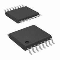
The DG611A, DG612A and DG613A are available in 16 lead
SOIC, TSSOP and the space saving 1.8 mm x 2.6 mm
miniQFN packages.
• Halogen-free according to IEC 61249-2-21
Definition
• Low charge injection (1 pC typ.)
• Leakage current < 0.25 nA at 85 °C
• Low switch capacitance (Csoff 2 pF typ.)
• Low RDS(on) - 115 max.
• Fully specified with single supply operation at 3 V, 5 V and
dual supplies at ± 5 V
• Low voltage, 2.5 V CMOS/TTL compatible
• 720 MHz, 3 dB bandwidth
• Excellent isolation performance (62 dB at 10 MHz)
• Excellent crosstalk performance (90 dB at 10 MHz)
• Fully specified from - 40 °C to + 85 °C and - 40 °C to + 125 °C
• 16 lead SOIC, TSSOP and miniQFN package (1.8 mm x 2.6 mm)
• Compliant to RoHS Directive 2002/95/EC
APPLICATIONS
•
•
•
•
•
•
•
Precision instrumentation
Medical instrumentation
Automated test equipment
High speed communications applications
High-end data acquisition
Sample and hold applications
Sample and hold systems
FUNCTIONAL BLOCK DIAGRAM AND PIN CONFIGURATION
DG611A
SOIC/TSSOP
DG611A
miniQFN
D1 IN1 IN2 D2
IN1
1
16
IN2
D1
2
15
D2
S1
3
14
S2
V-
4
13
V+
GND
5
12
NC
S4
6
11
S3
D4
7
10
D3
IN4
8
9
Top View
IN3
16
Kxx
Pin 1
14
13
S1
1
12
S2
V-
2
11
V+
GND
3
10
NC
S4
4
9
S3
5
Device Marking: Kxx for DG611A
(miniQFN16)
Lxx for DG612A
Pxx for DG613A
xx = Date/Lot Traceability Code
15
6
7
8
D4 IN4 IN3 D3
Top View
TRUTH TABLE
Logic
DG611A
DG612A
0
On
Off
1
Off
On
Document Number: 69904
S11-1066-Rev. C, 30-May-11
www.vishay.com
1
This document is subject to change without notice.
THE PRODUCTS DESCRIBED HEREIN AND THIS DOCUMENT ARE SUBJECT TO SPECIFIC DISCLAIMERS, SET FORTH AT www.vishay.com/doc?91000
�DG611A, DG612A, DG613A
Vishay Siliconix
FUNCTIONAL BLOCK DIAGRAM AND PIN CONFIGURATION
DG613A
SOIC/TSSOP
DG613A
miniQFN
D1 IN1 IN2 D2
16
15
14
13
IN1
1
16
IN2
D1
2
15
D2
S1
1
12
S2
S1
3
14
S2
V-
2
11
V+
V-
4
13
V+
GND
3
10
NC
GND
5
12
NC
S4
4
9
S3
S4
6
11
S3
D4
7
10
D3
5
6
7
8
D4 IN4 IN3 D3
IN4
8
9
IN3
Top View
Top View
Pxx
Pin 1
Device Marking: Pxx for DG613A
(miniQFN16)
TRUTH TABLE
Logic
SW1, SW4
SW2, SW3
0
Off
On
1
On
Off
ORDERING INFORMATION
Temp. Range
Package
Part Number
16-pin TSSOP
DG611AEQ-T1-E3
DG612AEQ-T1-E3
DG613AEQ-T1-E3
16-pin Narrow SOIC
DG611AEY-T1-E3
DG612AEY-T1-E3
DG613AEY-T1-E3
16-pin miniQFN
DG611AEN-T1-E4
DG612AEN-T1-E4
DG613AEN-T1-E4
DG611A, DG612A, DG613A
- 40 °C to 125 °Ca
Notes:
a. - 40 °C to 85 °C datasheet limits apply.
www.vishay.com
2
Document Number: 69904
S11-1066-Rev. C, 30-May-11
This document is subject to change without notice.
THE PRODUCTS DESCRIBED HEREIN AND THIS DOCUMENT ARE SUBJECT TO SPECIFIC DISCLAIMERS, SET FORTH AT www.vishay.com/doc?91000
�DG611A, DG612A, DG613A
Vishay Siliconix
ABSOLUTE MAXIMUM RATINGS (TA = 25 °C, unless otherwise noted)
Parameter
Limit
V + to V GND to V Digital
Inputsa
Unit
14
7
, VS, VD
Continuous Current (Any Terminal)
30
Peak Current, S or D (Pulsed 1 ms, 10 % Duty Cycle)
100
Storage Temperature
- 65 to 150
16-pin
Power Dissipation (Package)
V
(V -) - 0.3 V to (V +) + 0.3 V
or 30 mA, whichever occurs first
b
TSSOPc
16-pin miniQFN
16-pin Narrow
Thermal Resistance (Package)b
mA
°C
450
d
SOICe
525
mW
640
16-pin TSSOP
178
16-pin miniQFN
152
16-pin Narrow SOIC
125
°C/W
Notes:
a. Signals on SX, DX, or INX exceeding V + or V - will be clamped by internal diodes. Limit forward diode current to maximum current ratings.
b. All leads welded or soldered to PC Board.
c. Derate 5.6 mW/°C above 70 °C.
d. Derate 6.6 mW/°C above 70 °C.
e. Derate 8 mW/°C above 70 °C.
f. Manual soldering with iron is not recommended for leadless components. The miniQFN-16 is a leadless package. The end of the lead terminal
is exposed copper (not plated) as a result of the singulation process in manufacturing. A solder fillet at the exposed copper lip cannot be
guaranteed and is not required to ensure adequate bottom side solder interconnection.
Document Number: 69904
S11-1066-Rev. C, 30-May-11
www.vishay.com
3
This document is subject to change without notice.
THE PRODUCTS DESCRIBED HEREIN AND THIS DOCUMENT ARE SUBJECT TO SPECIFIC DISCLAIMERS, SET FORTH AT www.vishay.com/doc?91000
�DG611A, DG612A, DG613A
Vishay Siliconix
SPECIFICATIONS FOR DUAL SUPPLIES (V + = + 5 V, V - = - 5 V)
Test Conditions
Unless Otherwise Specified
V + = + 5 V, V - = - 5 V
VIN = 2 V, 0.8 Va
Temp.b
VANALOG
Full
RON
IS = 1 mA, VD = - 3 V, 0 V, + 3 V
Room
Full
72
115
160
115
140
RON
IS = 1 mA, VD = ± 3 V
Room
Full
0.7
4
6.5
4
5.5
RFLATNESS
IS = 1 mA, VD = - 3 V, 0 V, + 3 V
Room
Full
25
40
60
40
55
IS(off)
V + = 5.5 V, V - = - 5.5 V
VD = + 4.5 V/- 4.5 V
VS = - 4.5 V/+ 4.5 V
Room
Full
± 0.02
- 0.1
-2
0.1
2
- 0.1
- 0.25
0.1
0.25
Room
Full
± 0.02
- 0.1
-2
0.1
2
- 0.1
- 0.25
0.1
0.25
ID(on)
V + = 5.5 V, V - = - 5.5 V
VD = VS = ± 4.5 V
Room
Full
± 0.02
- 0.1
-6
0.1
6
- 0.1
- 0.25
0.1
0.25
Input Current, VIN Low
IIL
VIN Under Test = 0.8 V
Full
0.005
- 0.1
0.1
- 0.1
0.1
Input Current, VIN High
IIH
VIN Under Test = 2 V
Full
0.005
- 0.1
0.1
- 0.1
0.1
Input Capacitancee
CIN
f = 1 MHz
Room
2
Turn-On Time
tON
Room
Full
27
55
90
55
75
Turn-Off Time
tOFF
RL = 300 , CL = 35 pF
VS = ± 3 V, see figure 1
Room
Full
16
35
50
35
45
Break-Before-Make
Time Delay
tBBM
DG613A only, VS = 3 V
RL = 300 , CL = 35 pF
Room
Full
15
Q
Vg = 0 V, Rg = 0 , CL = 1 nF
Room
1
Room
- 62
Parameter
Symbol
- 40 °C to 125 °C - 40 °C to 85 °C
Typ.c
Min.d
Max.d
Min.d
5
-5
Max.d
Unit
5
V
Analog Switch
Analog Signal Rangee
On-Resistance
On-Resistance Match
On-Resistance Flatness
Switch Off
Leakage Current
ID(off)
Switch On
Leakage Current
-5
nA
Digital Control
µA
pF
Dynamic Characteristics
Charge Injection
e
2
Off Isolatione
OIRR
Channel-to-Channel
Crosstalke
XTALK
RL = 50 , CL = 5 pF
f = 10 MHz
Room
- 90
BW
RL = 50 , CL = 5 pF
Room
720
Room
2
Room
3
3 dB Bandwidthe
e
2
pC
dB
MHz
Source Off Capacitance
CS(off)
Drain Off Capacitancee
CD(off)
e
CD(on)
f = 1 MHz; VS = VD = 0 V
Room
9
THD
Signal = 1 VRMS, 20 Hz to 20 kHz,
RL = 600
Room
0.01
Room
Full
0.001
Room
Full
- 0.001
- 0.1
-1
- 0.1
-1
Room
Full
- 0.001
- 0.1
-1
- 0.1
-1
Drain On Capacitance
Total Harmonic
Distortione
f = 1 MHz; VS = 0 V
ns
pF
%
Power Supplies
Power Supply Current
I+
Negative Supply Current
I-
Ground Current
www.vishay.com
4
IGND
V + = + 5 V, V - = - 5 V
VIN = 0 V or 5 V
0.1
1
0.1
1
µA
Document Number: 69904
S11-1066-Rev. C, 30-May-11
This document is subject to change without notice.
THE PRODUCTS DESCRIBED HEREIN AND THIS DOCUMENT ARE SUBJECT TO SPECIFIC DISCLAIMERS, SET FORTH AT www.vishay.com/doc?91000
�DG611A, DG612A, DG613A
Vishay Siliconix
SPECIFICATIONS FOR UNIPOLAR SUPPLIES (V + = + 5 V, V - = 0 V)
Parameter
Symbol
Test Conditions
Unless Otherwise Specified
V + = + 5 V, V - = 0 V
VIN = 2 V, 0.8 Va
- 40 °C to 125 °C - 40 °C to 85 °C
Temp.b
Typ.c
Min.d
Max.d
Min.d
Max.d
Unit
0
5
0
5
V
Analog Switch
Analog Signal Rangee
VANALOG
Full
RON
V + = + 5 V, V - = 0 V
IS = 1 mA, VD = + 3.5 V
Room
Full
139
180
235
180
215
RON
V + = + 5 V, V - = 0 V,
IS = 1 mA, VD = + 3.5 V
Room
Full
1
6
10
6
9
RFLATNESS
V + = + 5 V, V - = 0 V,
IS = 1 mA, VD = 0 V, + 3.5 V
Room
Full
56
80
120
80
110
V + = 5.5 V, V - = 0 V
VD = 4.5 V/1 V
VS = 1 V/4.5 V
Room
Full
± 0.02
- 0.1
-2
0.1
2
- 0.1
- 0.25
0.1
0.25
Room
Full
± 0.02
- 0.1
-2
0.1
2
- 0.1
- 0.25
0.1
0.25
ID(on)
V + = 5.5 V, V - = 0 V
VD = VS = 1 V/4.5 V
Room
Full
± 0.02
- 0.1
-6
0.1
6
- 0.1
- 0.25
0.1
0.25
Input Current, VIN Low
IIL
VIN Under Test = 0.8 V
Full
0.005
- 0.1
0.1
- 0.1
0.1
Input Current, VIN High
IIH
VIN Under Test = 2 V
Full
0.005
- 0.1
0.1
- 0.1
0.1
Input Capacitancee
CIN
f = 1 MHz
Room
2
Turn-On Timee
tON
Room
Full
33
60
100
60
90
Turn-Off Timee
tOFF
RL = 300 , CL = 35 pF
VS = 3 V, see figure 1
Room
Full
16
35
50
35
45
Break-Before-Makee
Time Delay
tBBM
DG613A only, VS = 3 V
RL = 300 , CL = 35 pF
Room
Full
19
Injectione
Q
Vg = 0 V, Rg = 0 , CL = 1 nF
Full
2.3
e
OIRR
Room
- 61
Room
- 90
On-Resistance
On-Resistance Match
On-Resistance Flatness
Switch Off
Leakage Current
Switch On
Leakage Current
IS(off)
ID(off)
nA
Digital Control
µA
pF
Dynamic Characteristics
Charge
Off Isolation
Channel-to-Channel
Crosstalke
3 dB Bandwidthe
XTALK
RL = 50 , CL = 5 pF
f = 10 MHz
BW
RL = 50 , CL = 5 pF
Source Off Capacitancee
CS(off)
Drain Off Capacitancee
CD(off)
Drain On Capacitancee
CD(on)
f = 1 MHz; VS = 0 V
f = 1 MHz; VS = VD = 0 V
2
ns
2
pC
dB
Room
675
Room
3
MHz
Room
5
Room
9
Room
Full
0.001
Room
Full
- 0.001
- 0.1
-1
- 0.1
-1
Room
Full
- 0.001
- 0.1
-1
- 0.1
-1
pF
Power Supplies
Power Supply Current
I+
Negative Supply Current
I-
Ground Current
Document Number: 69904
S11-1066-Rev. C, 30-May-11
IGND
VIN = 0 V or 5 V
0.1
1
0.1
1
µA
www.vishay.com
5
This document is subject to change without notice.
THE PRODUCTS DESCRIBED HEREIN AND THIS DOCUMENT ARE SUBJECT TO SPECIFIC DISCLAIMERS, SET FORTH AT www.vishay.com/doc?91000
�DG611A, DG612A, DG613A
Vishay Siliconix
SPECIFICATIONS FOR UNIPOLAR SUPPLIES (V + = + 3 V, V - = 0 V)
- 40 °C to 125 °C - 40 °C to 85 °C
Test Conditions
Unless Otherwise Specified
V+ = + 3 V, V- = 0 V
VIN = 1.4 V, 0.6 Va
Temp.b
VANALOG
Full
RON
IS = 1 mA, VD = + 1.5 V
Room
Full
195
IS(off)
V + = 3.3 V, V- = 0 V
VD = 3 V/0.3 V
VS = 0.3 V/3 V
Room
Full
± 0.02
- 0.1
-2
0.1
2
- 0.1
- 0.25
0.1
0.25
Room
Full
± 0.02
- 0.1
-2
0.1
2
- 0.1
- 0.25
0.1
0.25
ID(on)
V + = 3.3 V, V- = 0 V
VD = VS = 0.3 V/3 V
Room
Full
± 0.02
- 0.1
-6
0.1
6
- 0.1
- 0.25
0.1
0.25
Input Current, VIN Low
IIL
VIN Under Test = 0.6 V
Full
0.005
- 0.1
0.1
- 0.1
0.1
Input Current, VIN High
IIH
VIN Under Test = 1.4 V
Full
0.005
- 0.1
0.1
- 0.1
0.1
Input Capacitancee
CIN
f = 1 MHz
Room
2
Room
Full
87
125
180
125
170
Room
Full
33
55
65
55
60
60
Parameter
Symbol
Typ.c
Min.d
Max.d
Min.d
3
0
Max.d
Unit
3
V
235
280
Analog Switch
Analog Signal Rangee
On-Resistance
Switch Off
Leakage Current
ID(off)
Switch On
Leakage Current
0
235
300
nA
Digital Control
µA
pF
Dynamic Characteristics
Turn-On Time
tON
Turn-Off Time
tOFF
Break-Before-Make
Time Delay
tBBM
DG613 only, VS = 2 V
RL = 300 , CL = 35 pF
Room
Full
Q
Vg = 0 V, Rg = 0 , CL = 1 nF
Room
2.3
Room
- 60
Charge
Injectione
RL = 300 , CL = 35 pF
VS = 2 V, see figure 1
10
Off Isolatione
OIRR
Channel-to-Channel
Crosstalke
XTALK
RL = 50 , CL = 5 pF
f = 10 MHz
Room
- 90
BW
RL = 50 , CL = 5 pF
Room
550
3 dB Bandwidthe
e
Source Off Capacitance
CD(off)
Capacitancee
CD(on)
Drain Off Capacitance
Drain On
CS(off)
e
f = 1 MHz; VS = 0 V
f = 1 MHz; VS = VD = 0 V
ns
10
pC
dB
MHz
Room
5
Room
6
Room
9
Room
Full
0.001
Room
Full
- 0.001
- 0.1
-1
- 0.1
-1
Room
Full
- 0.001
- 0.1
-1
- 0.1
-1
pF
Power Supplies
Power Supply Current
I+
Negative Supply Current
I-
Ground Current
IGND
VIN = 0 V or 3 V
0.1
1
0.1
1
µA
Notes:
a. VIN = input voltage to perform proper function.
b. Room = 25 °C, Full = as determined by the operating temperature suffix.
c. Typical values are for DESIGN AID ONLY, not guaranteed nor subject to production testing.
d. The algebraic convention whereby the most negative value is a minimum and the most positive a maximum, is used in this data sheet.
e. Guaranteed by design, not subject to production test.
Stresses beyond those listed under “Absolute Maximum Ratings” may cause permanent damage to the device. These are stress ratings only, and functional operation
of the device at these or any other conditions beyond those indicated in the operational sections of the specifications is not implied. Exposure to absolute maximum
rating conditions for extended periods may affect device reliability.
www.vishay.com
6
Document Number: 69904
S11-1066-Rev. C, 30-May-11
This document is subject to change without notice.
THE PRODUCTS DESCRIBED HEREIN AND THIS DOCUMENT ARE SUBJECT TO SPECIFIC DISCLAIMERS, SET FORTH AT www.vishay.com/doc?91000
�DG611A, DG612A, DG613A
Vishay Siliconix
TYPICAL CHARACTERISTICS (25 °C, unless otherwise noted)
250
600
V+ = 2.7 V
V± = ± 2.7 V
V± = ± 5 V
500
RON - On-Resistance ()
R ON - On-Resistance ()
200
150
100
50
V+ = 3 V
300
200
0
-6
-4
-2
0
2
4
6
8
0
2
VCOM (VD) - Analog Voltage (V)
180
180
160
160
R ON - On-Resistance ()
RON - On-Resistance ()
200
140
+ 125 °C
+ 85 °C
6
8
10
12
14
On-Resistance vs. VD (Single Supply)
200
120
4
VCOM (VD ) - Analog Voltage (V)
On-Resistance vs. VD (Dual Supply)
100
80
60
140
120
+ 125 °C
+ 85 °C
100
80
60
40
40
+ 25 °C
- 40 °C
20
0
-8
20
0
-6
-4
-2
0
2
4
6
0
8
2
4
6
8
10
12
14
VCOM (VD) - Analog Voltage (V)
On-Resistance vs. Temperature (Dual Supply)
10 000
On-Resistance vs. Temperature (Single Supply)
10 000
1000
100
IS (off)
V+ = 6.2 V
V- = - 6.2 V
10
0
20
40
60
100
IS (off)
V+ = 13.2 V
V- = 0 V
ID (off)
80
100
Temperature (°C)
Leakage Current vs. Temperature
Document Number: 69904
S11-1066-Rev. C, 30-May-11
ID (on)
10
ID (off)
- 20
Leakage Current (pA)
1000
ID (on)
1
- 40
+ 25 °C
- 40 °C
VCOM (VD) - Analog Voltage (V)
Leakage Current (pA)
V+ = 13.2 V
V+ = 5 V
100
V± = ± 6.2 V
0
-8
400
120
1
- 40
- 20
0
20
40
60
80
100
120
Temperature (°C)
Leakage Current vs. Temperature
www.vishay.com
7
This document is subject to change without notice.
THE PRODUCTS DESCRIBED HEREIN AND THIS DOCUMENT ARE SUBJECT TO SPECIFIC DISCLAIMERS, SET FORTH AT www.vishay.com/doc?91000
�DG611A, DG612A, DG613A
Vishay Siliconix
TYPICAL CHARACTERISTICS (25 °C, unless otherwise noted)
45
2.5
CL = 1nF
V+ = 3 V
40
t ON , tOFF - Switching Time (ns)
Q - Charge Injection (pC)
2.0
V+ = 5 V
1.5
1.0
V± = ± 5 V
0.5
35
tON V± = ± 5 V
30
25
20
15
tOFF V± = ± 5 V
10
5
0.0
-6
-4
-2
0
2
Analog Voltage (V)
4
0
- 40
6
Charge Injection vs. Analog Voltage
0
20
40
60
Temperature (°C)
80
100
120
Switching Time vs. Temperature (Dual Supply)
200
0
180
- 10
tON V+ = 3 V
160
140
120
100
tON V+ = 5 V
80
tOFF V+ = 5 V
60
Loss
- 20
Loss, OIRR, X TALK (dB)
t ON , tOFF - Switching Time (ns)
- 20
tOFF V+ = 3 V
40
- 30
- 40
- 50
OIRR
- 60
- 70
XTalk
- 80
- 90
- 100
20
V+ = 5.0 V
V- = - 5.0 V
R L = 50
- 110
0
- 40
- 20
0
20
40
60
80
Temperature (°C)
100
- 120
100K
120
Switching Time vs. Temperature (Single Supply)
1M
10M
Frequency (Hz)
100M
1G
Insertion Loss, Off-Isolation, Crosstalk
vs. Frequency
3.0
10 mA
- 40 °C to + 125 °C
1 mA
100 µA
2.0
Supply Current
VIN - Switching Threshold (V)
2.5
1.5
1.0
10 µA
1 µA
I100 nA
IGND
10 nA
1 nA
0.5
V+ = 5 V
V- = - 5 V
I+
100 pA
0.0
0
2
4
6
8
10
12
Switching Threshold vs. Supply Voltage
14
10 pA
10
100
1K
10K
100K
1M
10M
Switching Frequency (Hz)
Supply Current vs. Switching Frequency
www.vishay.com
8
Document Number: 69904
S11-1066-Rev. C, 30-May-11
This document is subject to change without notice.
THE PRODUCTS DESCRIBED HEREIN AND THIS DOCUMENT ARE SUBJECT TO SPECIFIC DISCLAIMERS, SET FORTH AT www.vishay.com/doc?91000
�DG611A, DG612A, DG613A
Vishay Siliconix
TEST CIRCUITS
+5V
tr < 5 ns
tf < 5 ns
3V
Logic
Input
50 %
0V
V+
VS
S
tOFF
D
Switch
Input*
VO
VS
VO
IN
RL
300
V-
GND
CL
35 pF
90 %
90 %
0V
tON
- 5V
Note:
CL (includes fixture and stray capacitance)
Logic input waveform is inverted for switches that
have the opposite logic sense control
RL
VO = V S
RL + rDS(on)
Figure 1. Switching Time
+5V
3V
Logic
Input
50 %
V+
VS1
S1
D1
VO1
IN1
VS2
Switch
Output
IN2
RL1
300
V-
GND
90 %
VO2
D2
S2
0V
VS1
VO1
RL2
300
CL2
35 pF
0V
VS2
VO2
CL1
35 pF
0V
Switch
Output
90 %
tD
tD
-5V
CL (includes fixture and stray capacitance)
Figure 2. Break-Before-Make (DG613A)
VO
+5V
Rg
INX
V+
S
ON
OFF
VO
CL
1 nF
3V
GND
OFF
D
IN
Vg
VO
V-
INX
OFF
ON
Q = VO x CL
OFF
-5V
Figure 3. Charge Injection
Document Number: 69904
S11-1066-Rev. C, 30-May-11
www.vishay.com
9
This document is subject to change without notice.
THE PRODUCTS DESCRIBED HEREIN AND THIS DOCUMENT ARE SUBJECT TO SPECIFIC DISCLAIMERS, SET FORTH AT www.vishay.com/doc?91000
�DG611A, DG612A, DG613A
Vishay Siliconix
TEST CIRCUITS
+5V
C
V+
D1
S1
VS
Rg = 50
50
IN1
0 V, 2.4 V
S2
D2
VO
NC
0 V, 2.4 V
RL
IN2
GND
XTALK Isolation = 20 log
V-
C
VO
-5V
VS
C = RF bypass
Figure 4. Crosstalk
+5V
+5V
C
V+
C
VO
D
S
VS
V+
Rg = 50
0 V, 2.4 V
S
RL
50
IN
GND
V-
Meter
IN
C
HP4192A
Impedance
Analyzer
or Equivalent
0 V, 2.4 V
D
-5V
Off Isolation = 20 log
GND
V-
C
VO
VS
C = RF Bypass
Figure 5. Off-Isolation
-5V
Figure 6. Source/Drain Capacitances
Vishay Siliconix maintains worldwide manufacturing capability. Products may be manufactured at one of several qualified locations. Reliability data for Silicon
Technology and Package Reliability represent a composite of all qualified locations. For related documents such as package/tape drawings, part marking, and
reliability data, see www.vishay.com/ppg?69904.
www.vishay.com
10
Document Number: 69904
S11-1066-Rev. C, 30-May-11
This document is subject to change without notice.
THE PRODUCTS DESCRIBED HEREIN AND THIS DOCUMENT ARE SUBJECT TO SPECIFIC DISCLAIMERS, SET FORTH AT www.vishay.com/doc?91000
�Package Information
www.vishay.com
Vishay Siliconix
Thin miniQFN16 Case Outline
B
12
0.10 C
Terminal tip (4)
16 x b
D
A
11
9
9
10
10
11
0.10 M C A B
0.05 M C
12
13
8
8
13
14
7
7
14
6
6
15
5
5
E
15
16
1
2
3
4
16
4
Pin #1 identifier (5)
15 x L
0.10 C
Top view
3
2
L1
1
e
Bottom view
0.10 C
C
A
Seating
plane
0.10 C
A3
Side view
DIMENSIONS
MILLIMETERS (1)
INCHES
MIN.
NOM.
MAX.
MIN.
NOM.
MAX.
A
0.50
0.55
0.60
0.020
0.022
0.024
A1
0
-
0.05
0
-
0.002
A3
0.15 ref.
b
0.15
D
2.50
e
0.006 ref.
0.20
0.25
0.006
2.60
2.70
0.098
0.40 BSC
E
1.70
1.80
0.008
0.010
0.102
0.106
0.016 BSC
1.90
0.067
0.071
0.075
L
0.35
0.40
0.45
0.014
0.016
0.018
L1
0.45
0.50
0.55
0.018
0.020
0.022
N (3)
16
16
Nd (3)
4
4
(3)
4
4
Ne
Notes
(1) Use millimeters as the primary measurement.
(2) Dimensioning and tolerances conform to ASME Y14.5M. - 1994.
(3) N is the number of terminals. Nd and Ne is the number of terminals in each D and E site respectively.
(4) Dimensions b applies to plated terminal and is measured between 0.15 mm and 0.30 mm from terminal tip.
(5) The pin 1 identifier must be existed on the top surface of the package by using identification mark or other feature of package body.
(6) Package warpage max. 0.05 mm.
ECN: T16-0226-Rev. B, 09-May-16
DWG: 6023
Revision: 09-May-16
Document Number: 64694
1
For technical questions, contact: analogswitchtechsupport@vishay.com
THIS DOCUMENT IS SUBJECT TO CHANGE WITHOUT NOTICE. THE PRODUCTS DESCRIBED HEREIN AND THIS DOCUMENT
ARE SUBJECT TO SPECIFIC DISCLAIMERS, SET FORTH AT www.vishay.com/doc?91000
�Package Information
Vishay Siliconix
SOIC (NARROW):
16ĆLEAD
JEDEC Part Number: MS-012
MILLIMETERS
16
15
14
13
12
11
10
Dim
A
A1
B
C
D
E
e
H
L
Ĭ
9
E
1
2
3
4
5
6
7
8
INCHES
Min
Max
Min
Max
1.35
1.75
0.053
0.069
0.10
0.20
0.004
0.008
0.38
0.51
0.015
0.020
0.18
0.23
0.007
0.009
9.80
10.00
0.385
0.393
3.80
4.00
0.149
0.157
1.27 BSC
0.050 BSC
5.80
6.20
0.228
0.244
0.50
0.93
0.020
0.037
0_
8_
0_
8_
ECN: S-03946—Rev. F, 09-Jul-01
DWG: 5300
H
D
C
All Leads
e
Document Number: 71194
02-Jul-01
B
A1
L
Ĭ
0.101 mm
0.004 IN
www.vishay.com
1
�Package Information
Vishay Siliconix
TSSOP: 16-LEAD
DIMENSIONS IN MILLIMETERS
Symbols
Min
Nom
Max
A
-
1.10
1.20
A1
0.05
0.10
0.15
A2
-
1.00
1.05
0.38
B
0.22
0.28
C
-
0.127
-
D
4.90
5.00
5.10
E
6.10
6.40
6.70
E1
4.30
4.40
4.50
e
-
0.65
-
L
0.50
0.60
0.70
L1
0.90
1.00
1.10
y
-
-
0.10
θ1
0°
3°
6°
ECN: S-61920-Rev. D, 23-Oct-06
DWG: 5624
Document Number: 74417
23-Oct-06
www.vishay.com
1
�PAD Pattern
www.vishay.com
Vishay Siliconix
RECOMMENDED MINIMUM PAD FOR TSSOP-16
0.193
(4.90)
0.171
0.014
0.026
0.012
(0.35)
(0.65)
(0.30)
(4.35)
(7.15)
0.281
0.055
(1.40)
Recommended Minimum Pads
Dimensions in inches (mm)
Revision: 02-Sep-11
1
Document Number: 63550
THIS DOCUMENT IS SUBJECT TO CHANGE WITHOUT NOTICE. THE PRODUCTS DESCRIBED HEREIN AND THIS DOCUMENT
ARE SUBJECT TO SPECIFIC DISCLAIMERS, SET FORTH AT www.vishay.com/doc?91000
�PAD Pattern
Vishay Siliconix
RECOMMENDED MINIMUM PADS FOR MINI QFN 16L
0.562
(0.0221)
0.400
(0.0157)
0.225
(0.0089)
1
2.900
(0.1142)
0.463
(0.0182)
1.200
(0.0472)
2.100
(0.0827)
Mounting Footprint
Dimensions in mm (inch)
Document Number: 66557
Revision: 05-Mar-10
www.vishay.com
1
�Application Note 826
Vishay Siliconix
RECOMMENDED MINIMUM PADS FOR SO-16
RECOMMENDED MINIMUM PADS FOR SO-16
0.372
(9.449)
0.152
0.022
0.050
0.028
(0.559)
(1.270)
(0.711)
(3.861)
0.246
(6.248)
0.047
(1.194)
Recommended Minimum Pads
Dimensions in Inches/(mm)
Return to Index
APPLICATION NOTE
Return to Index
www.vishay.com
24
Document Number: 72608
Revision: 21-Jan-08
�Legal Disclaimer Notice
www.vishay.com
Vishay
Disclaimer
ALL PRODUCT, PRODUCT SPECIFICATIONS AND DATA ARE SUBJECT TO CHANGE WITHOUT NOTICE TO IMPROVE
RELIABILITY, FUNCTION OR DESIGN OR OTHERWISE.
Vishay Intertechnology, Inc., its affiliates, agents, and employees, and all persons acting on its or their behalf (collectively,
“Vishay”), disclaim any and all liability for any errors, inaccuracies or incompleteness contained in any datasheet or in any other
disclosure relating to any product.
Vishay makes no warranty, representation or guarantee regarding the suitability of the products for any particular purpose or
the continuing production of any product. To the maximum extent permitted by applicable law, Vishay disclaims (i) any and all
liability arising out of the application or use of any product, (ii) any and all liability, including without limitation special,
consequential or incidental damages, and (iii) any and all implied warranties, including warranties of fitness for particular
purpose, non-infringement and merchantability.
Statements regarding the suitability of products for certain types of applications are based on Vishay's knowledge of typical
requirements that are often placed on Vishay products in generic applications. Such statements are not binding statements
about the suitability of products for a particular application. It is the customer's responsibility to validate that a particular product
with the properties described in the product specification is suitable for use in a particular application. Parameters provided in
datasheets and / or specifications may vary in different applications and performance may vary over time. All operating
parameters, including typical parameters, must be validated for each customer application by the customer's technical experts.
Product specifications do not expand or otherwise modify Vishay's terms and conditions of purchase, including but not limited
to the warranty expressed therein.
Hyperlinks included in this datasheet may direct users to third-party websites. These links are provided as a convenience and
for informational purposes only. Inclusion of these hyperlinks does not constitute an endorsement or an approval by Vishay of
any of the products, services or opinions of the corporation, organization or individual associated with the third-party website.
Vishay disclaims any and all liability and bears no responsibility for the accuracy, legality or content of the third-party website
or for that of subsequent links.
Except as expressly indicated in writing, Vishay products are not designed for use in medical, life-saving, or life-sustaining
applications or for any other application in which the failure of the Vishay product could result in personal injury or death.
Customers using or selling Vishay products not expressly indicated for use in such applications do so at their own risk. Please
contact authorized Vishay personnel to obtain written terms and conditions regarding products designed for such applications.
No license, express or implied, by estoppel or otherwise, to any intellectual property rights is granted by this document or by
any conduct of Vishay. Product names and markings noted herein may be trademarks of their respective owners.
© 2022 VISHAY INTERTECHNOLOGY, INC. ALL RIGHTS RESERVED
Revision: 01-Jan-2022
1
Document Number: 91000
�


 工商网监
湘ICP备2023018690号
工商网监
湘ICP备2023018690号
