DG9251, DG9252, DG9253
Vishay Siliconix
8-Channel, Dual 4-Channel, Triple 2-Channel Multiplexers
DESCRIPTION
FEATURES
The DG9251, DG9252, and DG9253 are high precision
single and dual supply CMOS analog multiplexers. DG9251
is an 8-channel multiplexer, the DG9252 is a dual 4-channel
multiplexer, and the DG9253 is a triple 2-channel multiplexer
or triple SPDT.
Designed to operate from a + 2.7 V to + 16 V single supply
or from a ± 2.7 V to ± 5 V dual supplies, the DG9251,
DG9252, and DG9253 are fully specified at + 16 V, + 5 V and
± 5 V. All control logic inputs have guaranteed 1.4 V high limit
when operating from + 5 V or ± 5 V supplies and 1.65 V when
operating from a + 16 V supply.
The DG9251, DG9252, and DG9253 are precision
multiplexers of low leakage, low charge injection, and
lowparasitic capacitance. They conduct equally well in
bothdirections, offer rail to rail analog signal handling and
can beused both as multiplexers as well as
de-multiplexers.The DG9251, DG9252, and DG9253
operating temperature is specified from - 40 °C to + 85 °C
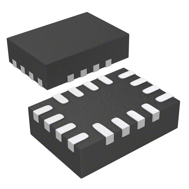
and are available in ultra compact 1.8 mm x 2.6 mm
miniQFN16 packages.
• Halogen-free According to IEC 61249-2-21
Definition
• + 2.7 V to + 16 V single supply operation
± 2.7 V to ± 5 V dual supply operation
• Fully specified at + 16 V, + 5 V, ± 5 V
• Low charge injection (< 4.1 pC typ.)
• High bandwidth: 314 MHz (DG9251)
449 MHz (DG9252)
480 MHz (DG9253)
• Low switch capacitance (Cs(off) 2.7 pF typ.)
• Good isolation and crosstalk performance
(typ. - 45 dB at 100 MHz)
• MiniQFN16 package (1.8 mm x 2.6 mm)
• Compliant to RoHS Directive 2002/95/EC
APPLICATIONS
•
•
•
•
•
•
Data acquisition
Medical and healthcare devices
Control and automation equipments
Test instruments
Touch panels
Consumer
FUNCTIONAL BLOCK DIAGRAM AND PIN CONFIGURATION
DG9251
mQFN-16
DG9253
mQFN-16
DG9252
mQFN-16
X6
X4
VCC
X2
Y2
Y0
VCC
X2
Y0
Y1
VCC
Y
16
15
14
13
16
15
14
13
16
15
14
13
X
1
12
X1
Y
1
12
X1
Z1
1
12
X
X7
2
11
X0
Y3
2
11
X
Z
2
11
X1
X5
3
10
X3
Y1
3
10
X0
Z0
3
10
X0
ENABLE
4
9
A
ENABLE
4
9
X3
ENABLE
4
9
A
Logic
Logic
5
6
77
8
5
6
7
8
5
6
77
8
VEE
GND
C
B
VEE
GND
B
A
VEE
GND
C
B
Top View
Top View
Yxx
Top View
Device Marking: 8xx for DG9251
(miniQFN16)
Hxx for DG9252
Jxx for DG9253
xx = Date/Lot Traceability Code
Pin 1
Document Number: 67075
S11-1550-Rev. C, 01-Aug-11
www.vishay.com
1
This document is subject to change without notice.
THE PRODUCTS DESCRIBED HEREIN AND THIS DOCUMENT ARE SUBJECT TO SPECIFIC DISCLAIMERS, SET FORTH AT www.vishay.com/doc?91000
�DG9251, DG9252, DG9253
Vishay Siliconix
TRUTH TABLE
Select Inputs
On Switches
Enable
Input
C
B
A
DG9251
DG9252
DG9253
H
X
X
X
All Switches Open
All Switches Open
All Switches Open
L
L
L
L
X to X0
X to X0, Y to Y0
X to X0, Y to Y0, Z to Z0
L
L
L
H
X to X1
X to X1, Y to Y1
X to X1, Y to Y0, Z to Z0
L
L
H
L
X to X2
X to X2, Y to Y2
X to X0, Y to Y1, Z to Z0
L
L
H
H
X to X3
X to X3, Y to Y3
X to X1, Y to Y1, Z to Z0
L
H
L
L
X to X4
X to X0, Y to Y0
X to X0, Y to Y0, Z to Z1
L
H
L
H
X to X5
X to X1, Y to Y1
X to X1, Y to Y0, Z to Z1
L
H
H
L
X to X6
X to X2, Y to Y2
X to X0, Y to Y1, Z to Z1
L
H
H
H
X to X7
X to X3, Y to Y3
X to X1, Y to Y1, Z to Z1
ORDERING INFORMATION
Temp. Range
Package
Part Number
DG9251, DG9252, DG9253
DG9251EN-T1-E4
- 40 °C to 125 °Ca
16-Pin miniQFN
DG9252EN-T1-E4
DG9253EN-T1-E4
Notes:
a. - 40 °C to 85 °C datasheet limits apply.
ABSOLUTE MAXIMUM RATINGS (TA = 25 °C, unless otherwise noted)
Parameter
Limit
VCC to VEE
18
GND to VDigital
Inputsa,
Unit
9
VS, VD
Continuous Current (Any terminal)
30
Peak Current, S or D (Pulsed 1 ms, 10 % duty cycle)
100
Storage Temperature
b
c, d
Power Dissipation
16-Pin miniQFN
Thermal Resistanceb
16-Pin miniQFNd
Latch-up (per JESD78)
V
(V-) - 0.3 to (V+) + 0.3
or 30 mA, whichever occurs first
mA
- 65 to 150
°C
525
mW
152
°C/W
> 300
mA
Notes:
a. Signals on SX, DX, or INX exceeding V+ or V- will be clamped by internal diodes. Limit forward diode current to maximum current ratings.
b. All leads welded or soldered to PC board.
c. Derate 6.6 mW/°C above 70 °C.
d. Manual soldering with iron is not recommended for leadless components. The miniQFN-16 is a leadless package. The end of the lead terminal
is exposed copper (not plated) as a result of the singulation process in manufacturing. A solder fillet at the exposed copper lip cannot be
guaranteed and is not required to ensure adequate bottom side solder interconnection.
www.vishay.com
2
Document Number: 67075
S11-1550-Rev. C, 01-Aug-11
This document is subject to change without notice.
THE PRODUCTS DESCRIBED HEREIN AND THIS DOCUMENT ARE SUBJECT TO SPECIFIC DISCLAIMERS, SET FORTH AT www.vishay.com/doc?91000
�DG9251, DG9252, DG9253
Vishay Siliconix
SPECIFICATIONS (for Dual Supplies)
Parameter
Test Conditions
Unless Otherwise Specified
VCC = + 5 V, VEE = - 5 V
VIN(A, B, C and ENABLE) = 1.4 V, 0.3 Va
Temp.b
VANALOG
Full
RON
IS = 1 mA, VD = - 3 V, 0 V, + 3 V
Room
Full
90
182
252
182
223
RON
IS = 1 mA, VD = ± 3 V
Room
Full
3.1
6
10
6
8
RFLATNESS
IS = 1 mA, VD = - 3 V, 0 V, + 3 V
Room
Full
32.4
44
64
44
61
Room
Full
± 0.02
-1
- 50
1
50
-1
-5
1
5
Room
Full
± 0.02
-1
- 50
1
50
-1
-5
1
5
Room
Full
± 0.02
-1
- 50
1
50
-1
-5
1
5
Symbol
- 40 °C to 125 °C - 40 °C to 85 °C
Typ.c
Min.d
Max.d
Min.d
5
-5
Max.d
Unit
5
V
Analog Switch
Analog Signal Rangee
On-Resistance
On-Resistance Match
On-Resistance Flatness
Switch Off
Leakage Current
Channel On
Leakage Current
IS(off)
ID(off)
ID(on)
VCC = 5.5 V, VEE = - 5.5 V,
VD = ± 4.5 V, VS = ± 4.5 V
VCC = 5.5 V, VEE = - 5.5 V,
VS = VD = ± 4.5 V
-5
nA
Digital Control
VIN(A, B, C and ENABLE) Low
VIL
Full
VIN(A, B, C and ENABLE) High
VIH
Full
Input Current, VIN Low
IIL
VIN(A, B, C and ENABLE)
under test = 0.3 V
Full
0.01
-1
1
-1
1
Input Current, VIN High
IIH
VIN(A, B, C and ENABLE)
under test = 1.4 V
Full
0.01
-1
1
-1
1
Input Capacitancee
CIN
f = 1 MHz
Room
2.4
Room
Full
88
236
281
236
251
Room
Full
158
250
455
250
369
Room
Full
40
125
136
125
131
Room
Full
32
f = 100 kHz
Room
< - 90
- 64
0.3
1.4
0.3
1.4
V
µA
pF
Dynamic Characteristics
Transition Time
tTRANS
Enable Turn-On Time
tON
Enable Turn-Off Time
tOFF
Break-Before-Make
Time Delay
Off Isolatione
RL = 300 , CL = 35 pF
see figure 1, 2, 3
tD
OIRR
RL = 50 , CL = 15 pF
Channel-to-Channel
Crosstalke
Bandwith, 3 dB
Charge Injectione
Source Off Capacitancee
Drain Off Capacitancee
Channel On Capacitancee
Total Harmonic
Distortione
Document Number: 67075
S11-1550-Rev. C, 01-Aug-11
XTALK
BW
Q
CS(off)
CD(off)
CD(on)
THD
RL = 50
f = 10 MHz
Room
f = 100 MHz
Room
- 45
f = 100 kHz
Room
< - 90
f = 10 MHz
Room
- 67
f = 100 MHz
Room
- 48
DG9251
Room
314
DG9252
Room
449
DG9253
Room
480
Vg = 0 V, Rg = 0 , CL = 1 nF
f = 1 MHz
f = 1 MHz
f = 1 MHz
13
Room
4.1
DG9251
Room
2.7
DG9252
Room
2.2
DG9253
Room
2.0
DG9251
Room
10.7
DG9252
Room
6.6
DG9253
Room
4.6
DG9251
Room
14.6
DG9252
Room
9.8
DG9253
Room
8.6
Room
0.2
Signal = 1 VRMS,
20 Hz to 20 kHz, RL = 600
ns
13
dB
MHz
pC
pF
%
www.vishay.com
3
This document is subject to change without notice.
THE PRODUCTS DESCRIBED HEREIN AND THIS DOCUMENT ARE SUBJECT TO SPECIFIC DISCLAIMERS, SET FORTH AT www.vishay.com/doc?91000
�DG9251, DG9252, DG9253
Vishay Siliconix
SPECIFICATIONS (for Dual Supplies)
Parameter
Symbol
Test Conditions
Unless Otherwise Specified
VCC = + 5 V, VEE = - 5 V
VIN(A, B, C and ENABLE) = 1.4 V, 0.3 Va
- 40 °C to 125 °C - 40 °C to 85 °C
Temp.b
Typ.c
Min.d
Max.d
Min.d
Room
Full
0.05
Room
Full
- 0.05
-1
- 10
-1
- 10
Room
Full
- 0.05
-1
- 10
-1
- 10
Max.d
Unit
Power Supplies
Power Supply Current
ICC
Negative Supply Current
IEE
Ground Current
VCC = + 5 V, VEE = - 5 V
VIN(A, B, C and ENABLE) = 0 or 5 V
IGND
1
10
1
10
µA
SPECIFICATIONS (for Unipolar Supplies)
Parameter
Symbol
Test Conditions
Unless Otherwise Specified
VCC = + 5 V, VEE = 0 V
VIN(A, B, C and ENABLE) = 1.4 V, 0.3 Va Temp.b
- 40 °C to 125 °C - 40 °C to 85 °C
Typ.c
Min.d
Max.d
Min.d
5
0
Max.d
Unit
5
V
Analog Switch
Analog Signal Rangee
On-Resistance
On-Resistance Match
On-Resistance Flatness
Switch Off
Leakage Current
Channel On
Leakage Current
VANALOG
Full
RON
IS = 1 mA, VD = 0 V, + 3.5 V
Room
Full
145
482
565
482
513
RON
IS = 1 mA, VD = + 3.5 V
Room
Full
3.6
20
22
20
21
RFLATNESS
IS = 1 mA, VD = 0 V, + 3 V
Room
Full
113
151
254
151
231
Room
Full
± 0.02
-1
- 50
1
50
-1
-5
1
5
Room
Full
± 0.02
-1
- 50
1
50
-1
-5
1
5
Room
Full
± 0.02
-1
- 50
1
50
-1
-5
1
5
IS(off)
ID(off)
ID(on)
VCC = + 5.5 V, VEE = 0 V
VD = 1 V/4.5 V, VS = 4.5 V/1 V
VCC = + 5.5 V, VEE = 0 V
VD = VS = 1 V/4.5 V
0
nA
Digital Control
VIN(A, B, C and ENABLE) Low
VIL
Full
VIN(A, B, C and ENABLE) High
VIH
Full
0.3
1.4
0.3
1.4
Input Current, VIN Low
IL
VIN(A, B, C and ENABLE)
under test = 0.3 V
Full
0.01
-1
1
-1
1
Input Current, VIN High
IH
VIN(A, B, C and ENABLE)
under test = 1.4 V
Full
0.01
-1
1
-1
1
Room
Full
97
V
µA
Dynamic Characteristics
Transition Time
tTRANS
Enable Turn-On Time
tON
Enable Turn-Off Time
tOFF
Break-Before-Make
Time Delay
tD
Charge Injectione
Q
Isolatione
OIRR
Off
Channel-to-Channel
Crosstalke
www.vishay.com
4
XTALK
RL = 300 , CL = 35 pF
see figure 1, 2, 3
Vg = 0 V, Rg = 0 , CL = 1 nF
RL = 50 , CL = 15 pF
f = 100 kHz
230
305
230
266
Room
Full
229
335
652
335
545
Room
Full
64
150
173
150
163
Room
Full
36
Full
0.44
Room
< - 90
Room
< - 90
20
ns
20
pC
dB
Document Number: 67075
S11-1550-Rev. C, 01-Aug-11
This document is subject to change without notice.
THE PRODUCTS DESCRIBED HEREIN AND THIS DOCUMENT ARE SUBJECT TO SPECIFIC DISCLAIMERS, SET FORTH AT www.vishay.com/doc?91000
�DG9251, DG9252, DG9253
Vishay Siliconix
SPECIFICATIONS (for Unipolar Supplies)
Parameter
Symbol
Test Conditions
Unless Otherwise Specified
VCC = + 5 V, VEE = 0 V
VIN(A, B, C and ENABLE) = 1.4 V, 0.3 Va Temp.b
- 40 °C to 125 °C - 40 °C to 85 °C
Typ.c
Min.d
Max.d
Min.d
Max.d
Unit
Dynamic Characteristics
Source Off Capacitancee
Drain Off Capacitancee
Channel On Capacitancee
CS(off)
CD(off)
CD(on)
f = 1 MHz
f = 1 MHz
f = 1 MHz
DG9251
Room
2.9
DG9252
Room
2.2
DG9253
Room
2.1
DG9251
Room
12.4
DG9252
Room
6.8
DG9253
Room
4.6
DG9251
Room
16
DG9252
Room
10.6
DG9253
Room
8.8
Room
Full
0.05
Room
Full
- 0.05
-1
- 10
-1
- 10
Room
Full
- 0.05
-1
- 10
-1
- 10
pF
Power Supplies
Power Supply Current
ICC
Negative Supply Current
IEE
Ground Current
VIN(A, B, C and ENABLE) = 0 V or 5 V
IGND
1
10
1
10
µA
SPECIFICATIONS (for Unipolar Supplies)
Parameter
Symbol
Test Conditions
Unless Otherwise Specified
VCC = + 16 V, VEE = 0 V
VIN(A, B, C and ENABLE) = 1.6 V, 0.5 Va Temp.b
- 40 °C to 125 °C - 40 °C to 85 °C
Typ.c
Min.d
Max.d
Min.d
16
0
Max.d
Unit
Analog Switch
Analog Signal Rangee
On-Resistance
On-Resistance Match
On-Resistance Flatness
Switch Off
Leakage Current
Channel On
Leakage Current
VANALOG
Full
16
V
RON
IS = 1 mA, VD = 0.7 V, 8 V, 15.3 V
Room
Full
69
152
171
152
158
RON
IS = 1 mA, VD = + 0.7 V
Room
Full
2
7
10
7
8
RFLATNESS
IS = 1 mA, VD = 0.7 V, + 15.3 V
Room
Full
32
45
53
45
49
Room
Full
± 0.02
-1
- 50
1
50
-1
-5
1
5
Room
Full
± 0.02
-1
- 50
1
50
-1
-5
1
5
Room
Full
± 0.02
-1
- 50
1
50
-1
-5
1
5
IS(off)
ID(off)
ID(on)
VCC = + 16 V, VEE = 0 V
VD = 1 V/15 V, VS = 15 V/1 V
VCC = + 16 V, VEE = 0 V
VD = VS = 1 V/15 V
0
nA
Digital Control
VIN(A, B, C and ENABLE) Low
VIL
Full
VIN(A, B, C and ENABLE) High
VIH
Full
0.5
1.6
0.5
1.6
Input Current, VIN Low
IL
VIN(A, B, C and ENABLE)
under test = 0.5 V
Full
0.01
-1
1
-1
1
Input Current, VIN High
IH
VIN(A, B, C and ENABLE)
under test = 1.6 V
Full
0.01
-1
1
-1
1
Room
Full
56
130
160
130
150
Room
Full
98
175
256
175
221
Room
Full
37
120
134
120
127
Room
Full
31
V
µA
Dynamic Characteristics
Transition Time
tTRANS
Enable Turn-On Time
tON
Enable Turn-Off Time
tOFF
Break-Before-Make
Time Delay
Document Number: 67075
S11-1550-Rev. C, 01-Aug-11
tD
RL = 300 , CL = 35 pF
see figure 1, 2, 3
12
ns
12
www.vishay.com
5
This document is subject to change without notice.
THE PRODUCTS DESCRIBED HEREIN AND THIS DOCUMENT ARE SUBJECT TO SPECIFIC DISCLAIMERS, SET FORTH AT www.vishay.com/doc?91000
�DG9251, DG9252, DG9253
Vishay Siliconix
SPECIFICATIONS (for Unipolar Supplies)
Parameter
Symbol
Charge Injection
e
Test Conditions
Unless Otherwise Specified
VCC = + 16 V, VEE = 0 V
VIN(A, B, C and ENABLE) = 1.6 V, 0.5 Va Temp.b
Vg = 0 V, Rg = 0 , CL = 1 nF
Q
- 40 °C to 125 °C - 40 °C to 85 °C
Typ.c
Room
4.5
Room
< - 90
Room
< - 90
Min.d
Max.d
Min.d
Max.d
Unit
pC
Dynamic Characteristics
Off Isolatione
OIRR
Channel-to-Channel
Crosstalke
XTALK
RL = 50 , CL = 15 pF
f = 100 kHz
Source Off Capacitancee
CS(off)
f = 1 MHz
Drain Off Capacitancee
Channel On Capacitancee
CD(off)
f = 1 MHz
CD(on)
f = 1 MHz
dB
DG9251
Room
2.6
DG9252
Room
2.1
DG9253
Room
1.8
DG9251
Room
10.4
DG9252
Room
5.8
DG9253
Room
4.2
DG9251
Room
15
DG9252
Room
9.5
DG9253
Room
8.2
Room
Full
0.05
Room
Full
- 0.05
-1
- 10
-1
- 10
Room
Full
- 0.05
-1
- 10
-1
- 10
pF
Power Supplies
Power Supply Current
ICC
Negative Supply Current
IEE
VIN(A, B, C and ENABLE) = 0 V or 16 V
IGND
Ground Current
1
10
1
10
µA
Notes:
a. VIN = input voltage to perform proper function.
b. Room - 25 °C, full = as determined by the operating temperature suffix.
c. Typical values are for DESIGN AID ONLY, not guaranteed nor subject to production testing.
d. The algebraic convention whereby the most negative value is a minimum and the most positive a maximum, is used in this datasheet.
e. Guaranteed by design, not subject to production test.
Stresses beyond those listed under “Absolute Maximum Ratings” may cause permanent damage to the device. These are stress ratings only, and functional operation
of the device at these or any other conditions beyond those indicated in the operational sections of the specifications is not implied. Exposure to absolute maximum
rating conditions for extended periods may affect device reliability.
TYPICAL CHARACTERISTICS (25 °C, unless otherwise noted)
700
250
T = 25 °C
IS = 1 mA
600
T = 25 °C
IS = 1 mA
RON - On-Resistance (Ω)
RON - On-Resistance (Ω)
200
500
VCC = 3 V
400
300
VCC = 5 V
200
VCC = 12 V
VCC = + 2.7 V
VEE = - 2.7 V
150
VCC = + 5 V
VEE = - 5 V
100
50
100
VCC = 16 V
0
0
0
2
4
6
8
10
12
VD - Analog Voltage (V)
14
16
RON vs. VD and Single Supply Voltage
www.vishay.com
6
VCC = + 6.2 V
VEE = - 6.2 V
VCC = + 8 V
VEE = - 8 V
-8
-6
-4
-2
0
2
4
6
8
VD - Analog Voltage (V)
RON vs. VD and Dual Supply Voltage
Document Number: 67075
S11-1550-Rev. C, 01-Aug-11
This document is subject to change without notice.
THE PRODUCTS DESCRIBED HEREIN AND THIS DOCUMENT ARE SUBJECT TO SPECIFIC DISCLAIMERS, SET FORTH AT www.vishay.com/doc?91000
�DG9251, DG9252, DG9253
Vishay Siliconix
TYPICAL CHARACTERISTICS (25 °C, unless otherwise noted)
200
350
VCC = 5 V, VEE = 0 V
IS = 1 mA
250
T = 85 °C
T = 125 °C
200
150
T = 25 °C
100
50
2
3
VD - Analog Voltage (V)
4
5
100
75
T = 25 °C
50
T = - 40 °C
-3
-2
-1
0
1
2
3
4
5
RON vs. Analog Voltage and Temperature
140
160
VCC = 12 V, VEE = 0 V
IS = 1 mA
140
VCC = 16 V, VEE = 0 V
IS = 1 mA
120
T = 125 °C
T = 85 °C
120
RON - On-Resistance (Ω)
RON - On-Resistance (Ω)
-4
VD - Analog Voltage (V)
RON vs. Analog Voltage and Temperature
T = 125 °C
100
80
60
T = 25 °C
40
T = 85 °C
100
80
60
T = 25 °C
40
T = - 40 °C
T = - 40 °C
20
20
0
0
0
1
2
3
4
5
6
7
8
9
0
10 11 12
2
4
VD - Analog Voltage (V)
RON vs. Analog Voltage and Temperature
6
8
10
12
VD - Analog Voltage (V)
14
16
RON vs. Analog Voltage and Temperature
10 000
10 000
VCC = + 16 V
VEE = 0 V
VCC = + 5.5 V
VEE = - 5.5 V
1000
Leakage Current (pA)
1000
Leakage Current (pA)
T = 85 °C
T = 125 °C
125
0
-5
0
1
150
25
T = - 40 °C
0
VCC = 5 V, VEE = - 5 V
IS = 1 mA
175
RON - On-Resistance (Ω)
RON - On-Resistance (Ω)
300
100
IS(OFF)
10
ID(OFF)
1
- 60 - 40 - 20
ID(ON)
0
20
40
60
80
100 120 140
Temperature (°C)
Leakage Current vs. Temperature
Document Number: 67075
S11-1550-Rev. C, 01-Aug-11
IS(OFF)
100
ID(ON)
ID(OFF)
10
1
- 60 - 40 - 20
0
20 40 60 80
Temperature (°C)
100 120 140
Leakage Current vs. Temperature
www.vishay.com
7
This document is subject to change without notice.
THE PRODUCTS DESCRIBED HEREIN AND THIS DOCUMENT ARE SUBJECT TO SPECIFIC DISCLAIMERS, SET FORTH AT www.vishay.com/doc?91000
�DG9251, DG9252, DG9253
Vishay Siliconix
TYPICAL CHARACTERISTICS
0
20
- 10
Loss
QINJ - Charge Injection (pC)
Loss, OIRR, XTALK (dB)
- 20
VCC = + 5 V
VEE = - 5 V
RL = 50 Ω
- 30
- 40
- 50
OIRR
- 60
XTALK
- 70
- 80
15
10
VCC = 5 V
VEE = 0 V
5
VCC = 16 V
VEE = 0 V
VCC = 3 V
VEE = 0 V
0
- 90
- 100
100K
1M
10M
100M
-5
1G
VCC = 12 V
VEE = 0 V
VCC = 5 V
VEE = - 5 V
-5
-3
-1
1
3
5
7
9
11
13
15
Frequency (Hz)
VS - Analog Voltage (V)
DG9251 Insertion Loss, Off-Isolation, Crosstalk vs. Frequency
DG9251 Charge Injection vs. Analog Voltage
0
15
Loss
- 10
VCC = 16 V
- 30
QINJ - Charge Injection (pC)
Loss, OIRR, XTALK (dB)
- 20
VCC = + 5 V
VEE = - 5 V
- 40
- 50
OIRR
- 60
XTALK
- 70
- 80
10
VCC = 5 V
5
VCC = 3 V
VCC = 12 V
0
VCC = 5 V
- 90
- 100
100K
1M
10M
100M
-5
-6
1G
-4
-2
0
Frequency (Hz)
DG9252 Insertion Loss, Off-Isolation, Crosstalk vs. Frequency
14
16
15
Loss
VCC = 16 V
QINJ - Charge Injection (pC)
- 20
Loss, OIRR, XTALK (dB)
12
DG9252 Charge Injection vs. Analog Voltage
0
- 10
- 30
2
4
6
8 10
VS - Analog Voltage (V)
VCC = + 5 V
VEE = - 5 V
- 40
- 50
OIRR
- 60
- 70
XTALK
- 80
10
VCC = 5 V
5
VCC = 3 V
VCC = 12 V
0
VCC = 5 V
- 90
- 100
100K
1M
10M
100M
1G
-5
-6
-4
-2
0
2
4
6
8
10
12
14
16
Frequency (Hz)
VS - Analog Voltage (V)
DG9253 Insertion Loss, Off-Isolation, Crosstalk vs. Frequency
DG9253 Charge Injection vs. Analog Voltage
www.vishay.com
8
Document Number: 67075
S11-1550-Rev. C, 01-Aug-11
This document is subject to change without notice.
THE PRODUCTS DESCRIBED HEREIN AND THIS DOCUMENT ARE SUBJECT TO SPECIFIC DISCLAIMERS, SET FORTH AT www.vishay.com/doc?91000
�DG9251, DG9252, DG9253
Vishay Siliconix
TYPICAL CHARACTERISTICS
1.7
VCC = 16 V, VEE = 0 V, tOFF
220
1.5
VCC = 5 V, VEE = - 5 V, tON
300
260
- 40 °C to + 125 °C
VCC = 5 V, VEE = 0 V, tON
340
VT - Switching Threshold (V)
tON(EN), tOFF(EN) - Switching Time (ns)
380
VCC = 16 V,
VEE = 0 V, tON
VCC = 5 V,
VEE = - 5 V, tOFF
VCC = 5 V,
VEE = 0 V, tOFF
180
140
100
VIH
1.1
VIL
0.9
0.7
0.5
60
20
- 40
1.3
- 20
0
20
40
60
80
100
120
0.3
140
2
4
6
Temperature (°C)
Switching Time vs. Temperature
8
10
12
14
VCC - Supply Voltage (V)
16
18
Switching Threshold vs. Supply Voltage
10 000
ICC - Supply Current (µA)
1000
ICC
VCC = + 5 V
VEE = - 5 V
100
10
1
IGND
IEE
0.1
0.01
0.001
0.0001
10
100
1K
10K
100K
1M
10M
Input Switching Frequency (Hz)
Supply Current vs. Input Switching Frequency
Document Number: 67075
S11-1550-Rev. C, 01-Aug-11
www.vishay.com
9
This document is subject to change without notice.
THE PRODUCTS DESCRIBED HEREIN AND THIS DOCUMENT ARE SUBJECT TO SPECIFIC DISCLAIMERS, SET FORTH AT www.vishay.com/doc?91000
�DG9251, DG9252, DG9253
Vishay Siliconix
TEST CIRCUITS
VCC
1.8 V
VCC
50 Ω
X0
A
B
C
VX0
VA, B, C
50 %
0V
X1 - X6
DG9251
X7
90 %
VO
X
ENABLE
GND
VX0 or VY0 or VZ0
VX7
VEE
300 Ω
35 pF
VO
50 %
VX7
VX3 or VY3
VX1 or VY1 or VZ1
t TRANS
VEE
VCC
VCC
X0 or Y0
VX0 or VY0
X1 - X2 or
Y1 - Y2
DG9252
X3 or Y3
VX3 or VY3
A
B
50 Ω
ENABLE
GND
X7 on DG9251
X3 or Y3 on DG9252
X1 or Y1 or Z1 on DG9253
t TRANS
VO
X or Y
VEE
90 %
300 Ω
35 pF
VEE
VCC
VCC
X0 or Y0
or Z0
VX0 or VY0 or VZ0
X1 or Y1 or Z1
VX1 or VY1 or VZ1
A or B
or C
50 Ω
DG9253
ENABLE
GND
VO
X or Y or Z
VEE
300 Ω
35 pF
VEE
Figure 1. Transition Time
www.vishay.com
10
Document Number: 67075
S11-1550-Rev. C, 01-Aug-11
This document is subject to change without notice.
THE PRODUCTS DESCRIBED HEREIN AND THIS DOCUMENT ARE SUBJECT TO SPECIFIC DISCLAIMERS, SET FORTH AT www.vishay.com/doc?91000
�DG9251, DG9252, DG9253
Vishay Siliconix
TEST CIRCUITS
VCC
1.8 V
VCC
A
B
C
X0
VCC
VENABLE
X1 - X7
DG9251
VX0 or VY0 or VZ0
VEE
GND
VO
X
ENABLE
50 Ω
50 %
0V
300 Ω
90 %
VO
35 pF
50 %
90 %
0V
tON
t OFF
VEE
Enable X or Y or Z
Disable X or Y or Z
VCC
VCC
X0 or Y0
A
B
VCC
X1 - X3 or
Y1 - Y3
DG9252
50 Ω
VEE
GND
VO
X or Y
ENABLE
300 Ω
35 pF
VEE
VCC
VCC
X0 or Y0
or Z0
A or B
or C
VCC
X1 or Y1 or Z1
DG9253
ENABLE
50 Ω
GND
VO
X or Y or Z
VEE
300 Ω
35 pF
VEE
Figure 2. Enable Switching Time
Document Number: 67075
S11-1550-Rev. C, 01-Aug-11
www.vishay.com
11
This document is subject to change without notice.
THE PRODUCTS DESCRIBED HEREIN AND THIS DOCUMENT ARE SUBJECT TO SPECIFIC DISCLAIMERS, SET FORTH AT www.vishay.com/doc?91000
�DG9251, DG9252, DG9253
Vishay Siliconix
TEST CIRCUITS
VCC
1.8 V
VCC
50 Ω
X0 - X7
A
B
C
VCC
VA, B, C
DG9251
50 %
0V
VX0 or VY0 or VZ0
80 %
GND
VO
X
ENABLE
VEE
300 Ω
VO
35 pF
0V
tD
VEE
VCC
VCC
A
B
X0 - X3 or
Y0- Y3
VCC
50 Ω
DG9252
GND
VO
X or Y
ENABLE
VEE
300 Ω
35 pF
VEE
VCC
VCC
X0, X1 or Y0,
Y1 or Z0, Z1
A or B
or C
VCC
50 Ω
DG9253
ENABLE
GND
VO
X or Y or Z
VEE
300 Ω
35 pF
VEE
Figure 3. Break-Before-Make
www.vishay.com
12
Document Number: 67075
S11-1550-Rev. C, 01-Aug-11
This datasheet is subject to change without notice.
THE PRODUCT DESCRIBED HEREIN AND THIS DATASHEET ARE SUBJECT TO SPECIFIC DISCLAIMERS, SET FORTH AT www.vishay.com/doc?91000
�DG9251, DG9252, DG9253
Vishay Siliconix
TEST CIRCUITS
VCC
tr < 5 ns
tf < 5 ns
VCC
VCC
A
B
C
Channel
Select
ON
OFF
VENABLE
OFF
0V
Rg
Xx
VO
Vg
VEE
GND
ΔVO
VO
X
ENABLE
1 nF
VEE
Figure 4. Charge Injection
VCC
VCC
Network Analyzer
Network Analyzer
VCC
VCC
VIN
A
B
C
A
B
C
X0
Rg = 50 Ω
Vg
VOUT
X
ENABLE
VCC
V EE
GND
VIN
X0
Vg
VOUT
X
ENABLE
VEE
GND
50 Ω
Rg = 50 Ω
50 Ω
VEE
V EE
Insertion Loss = 20 log
Off Isolation = 20 log
VOUT
VIN
Figure 5. Insertion Loss
VOUT
VIN
Figure 6. Off Isolation
VCC
VCC
Network Analyzer
VCC
A
B
C
VIN
X0
Vg
Rg = 50 Ω
VCC
Channel
Select
A
B
C
X0
|
to
|
Xx
X
50 Ω
GND
VOUT
Xx
ENABLE
VEE
50 Ω
ENABLE
GND
Impedance
Analyzer
X
VEE
VEE
Crosstalk = 20 log
VOUT
VIN
Figure 7. Crosstalk
VEE
Figure 8. Source, Drain Capacitance
Vishay Siliconix maintains worldwide manufacturing capability. Products may be manufactured at one of several qualified locations. Reliability data for Silicon
Technology and Package Reliability represent a composite of all qualified locations. For related documents such as package/tape drawings, part marking, and
reliability data, see www.vishay.com/ppg?67075.
Document Number: 67075
S11-1550-Rev. C, 01-Aug-11
www.vishay.com
13
�Package Information
www.vishay.com
Vishay Siliconix
Thin miniQFN16 Case Outline
B
12
0.10 C
Terminal tip (4)
16 x b
D
A
11
9
9
10
10
11
0.10 M C A B
0.05 M C
12
13
8
8
13
14
7
7
14
6
6
15
5
5
E
15
16
1
2
3
4
16
4
Pin #1 identifier (5)
15 x L
0.10 C
Top view
3
2
L1
1
e
Bottom view
0.10 C
C
A
Seating
plane
0.10 C
A3
Side view
DIMENSIONS
MILLIMETERS (1)
INCHES
MIN.
NOM.
MAX.
MIN.
NOM.
MAX.
A
0.50
0.55
0.60
0.020
0.022
0.024
A1
0
-
0.05
0
-
0.002
A3
0.15 ref.
b
0.15
D
2.50
e
0.006 ref.
0.20
0.25
0.006
2.60
2.70
0.098
0.40 BSC
E
1.70
1.80
0.008
0.010
0.102
0.106
0.016 BSC
1.90
0.067
0.071
0.075
L
0.35
0.40
0.45
0.014
0.016
0.018
L1
0.45
0.50
0.55
0.018
0.020
0.022
N (3)
16
16
Nd (3)
4
4
(3)
4
4
Ne
Notes
(1) Use millimeters as the primary measurement.
(2) Dimensioning and tolerances conform to ASME Y14.5M. - 1994.
(3) N is the number of terminals. Nd and Ne is the number of terminals in each D and E site respectively.
(4) Dimensions b applies to plated terminal and is measured between 0.15 mm and 0.30 mm from terminal tip.
(5) The pin 1 identifier must be existed on the top surface of the package by using identification mark or other feature of package body.
(6) Package warpage max. 0.05 mm.
ECN: T16-0226-Rev. B, 09-May-16
DWG: 6023
Revision: 09-May-16
Document Number: 64694
1
For technical questions, contact: analogswitchtechsupport@vishay.com
THIS DOCUMENT IS SUBJECT TO CHANGE WITHOUT NOTICE. THE PRODUCTS DESCRIBED HEREIN AND THIS DOCUMENT
ARE SUBJECT TO SPECIFIC DISCLAIMERS, SET FORTH AT www.vishay.com/doc?91000
�PAD Pattern
Vishay Siliconix
RECOMMENDED MINIMUM PADS FOR MINI QFN 16L
0.562
(0.0221)
0.400
(0.0157)
0.225
(0.0089)
1
2.900
(0.1142)
0.463
(0.0182)
1.200
(0.0472)
2.100
(0.0827)
Mounting Footprint
Dimensions in mm (inch)
Document Number: 66557
Revision: 05-Mar-10
www.vishay.com
1
�Legal Disclaimer Notice
www.vishay.com
Vishay
Disclaimer
ALL PRODUCT, PRODUCT SPECIFICATIONS AND DATA ARE SUBJECT TO CHANGE WITHOUT NOTICE TO IMPROVE
RELIABILITY, FUNCTION OR DESIGN OR OTHERWISE.
Vishay Intertechnology, Inc., its affiliates, agents, and employees, and all persons acting on its or their behalf (collectively,
“Vishay”), disclaim any and all liability for any errors, inaccuracies or incompleteness contained in any datasheet or in any other
disclosure relating to any product.
Vishay makes no warranty, representation or guarantee regarding the suitability of the products for any particular purpose or
the continuing production of any product. To the maximum extent permitted by applicable law, Vishay disclaims (i) any and all
liability arising out of the application or use of any product, (ii) any and all liability, including without limitation special,
consequential or incidental damages, and (iii) any and all implied warranties, including warranties of fitness for particular
purpose, non-infringement and merchantability.
Statements regarding the suitability of products for certain types of applications are based on Vishay's knowledge of typical
requirements that are often placed on Vishay products in generic applications. Such statements are not binding statements
about the suitability of products for a particular application. It is the customer's responsibility to validate that a particular product
with the properties described in the product specification is suitable for use in a particular application. Parameters provided in
datasheets and / or specifications may vary in different applications and performance may vary over time. All operating
parameters, including typical parameters, must be validated for each customer application by the customer's technical experts.
Product specifications do not expand or otherwise modify Vishay's terms and conditions of purchase, including but not limited
to the warranty expressed therein.
Hyperlinks included in this datasheet may direct users to third-party websites. These links are provided as a convenience and
for informational purposes only. Inclusion of these hyperlinks does not constitute an endorsement or an approval by Vishay of
any of the products, services or opinions of the corporation, organization or individual associated with the third-party website.
Vishay disclaims any and all liability and bears no responsibility for the accuracy, legality or content of the third-party website
or for that of subsequent links.
Except as expressly indicated in writing, Vishay products are not designed for use in medical, life-saving, or life-sustaining
applications or for any other application in which the failure of the Vishay product could result in personal injury or death.
Customers using or selling Vishay products not expressly indicated for use in such applications do so at their own risk. Please
contact authorized Vishay personnel to obtain written terms and conditions regarding products designed for such applications.
No license, express or implied, by estoppel or otherwise, to any intellectual property rights is granted by this document or by
any conduct of Vishay. Product names and markings noted herein may be trademarks of their respective owners.
© 2022 VISHAY INTERTECHNOLOGY, INC. ALL RIGHTS RESERVED
Revision: 01-Jan-2022
1
Document Number: 91000
�


 工商网监
湘ICP备2023018690号
工商网监
湘ICP备2023018690号
