DG9431E
www.vishay.com
Vishay Siliconix
1 pC Charge Injection, 100 pA Maximum Leakage, +5 V / +3 V,
SPDT Analog Switch
DESCRIPTION
FEATURES
The DG9431E is a monolithic CMOS switch designed for
precision signal switching. The 17 low voltage part
exhibits low charge injection over the full signal range, low
leakage, low parasitic capacitance, and fast switching.
• 1 pC charge injection
The DG9431E can switch both analog and digital signals.
Each switch conducts equally well in both directions when
on, and blocks up to the power supply level when off.
Break-before-make switching is guaranteed.
The DG9431E offers 1 nW typical power consumption and
8 kV ESD (HBM), 1 kV ESD (CDM) tolerance. It is ideal for
use in low voltage instruments and healthcare devices,
fitting the circuits of low voltage ADC and DAC, sample and
hold, analog front end gain control, and signal path
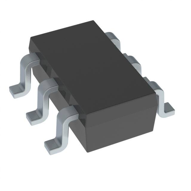
switching. The DG9431E is available in 6-lead TSOP and
8-lead SOIC packages.
• Guaranteed 100 pA max. switch on leakage at
25 °C
• 3.8 pF switch off and 7.8 pF switch on
capacitances
Available
Available
• +2.7 V to +5 V single supply operation
• Low on-resistance - RDS(on): 17 (typ.) at 5 V
• tON: 32 ns, tOFF: 10 ns switching time
• Typical power consumption: 1 nW
• Over voltage tolerance on logic control IN pin
• TTL / CMOS compatible
• ESD (HBM): > 8000 V, ESD (CDM): >1000 V
• Latch-up current: > 300 mA (JESD78)
• Available in TSOP-6 and SOIC-8
APPLICATIONS
Note
* This datasheet provides information about parts that are
RoHS-compliant and / or parts that are non-RoHS-compliant. For
example, parts with lead (Pb) terminations are not RoHS-compliant.
Please see the information / tables in this datasheet for details.
• Automatic test equipment
• Process control and automation
• Data acquisition systems
• Meters and instruments
BENEFITS
• Medical and healthcare systems
• Low charge injection and leakage
• Communication systems
• Low parasitic capacitance
• Sample-and-hold systems
• Fast switching speed
• Relay replacements
• High ESD tolerance
• Battery powered systems
FUNCTIONAL BLOCK DIAGRAM AND PIN CONFIGURATION
SOIC-8
TSOP-6
IN
V+
GND
1
6
2
5
4
3
NO
COM
NO
1
8
V+
COM
2
7
IN
LOGIC
NC
NO
NC
3
6
*
0
ON
OFF
GND
4
5
*
1
OFF
ON
NC
Top View
Top View
*Not Connected
TRUTH TABLE
Note
• Logic “0” 0.8 V
Logic “1” 2.4 V
ORDERING INFORMATION
TEMP. RANGE
-40 °C to +85 °C
CONFIGURATION
DG9431E
S16-2242–Rev. A, 31-Oct-16
PART NUMBER
PACKAGE
MINIUM ORDER / PACKAGING QUANTITY
6-pin TSOP
DG9431EDV-T1-GE3
Tape and reel 3000 units
DG9431EDY-T1-GE3
Tape and reel 2500 units
DG9431EDY-GE3
Tube 500 units
8-pin SOIC
Document Number: 76459
1
For technical questions, contact: analogswitchtechsupport@vishay.com
THIS DOCUMENT IS SUBJECT TO CHANGE WITHOUT NOTICE. THE PRODUCTS DESCRIBED HEREIN AND THIS DOCUMENT
ARE SUBJECT TO SPECIFIC DISCLAIMERS, SET FORTH AT www.vishay.com/doc?91000
�DG9431E
www.vishay.com
Vishay Siliconix
ABSOLUTE MAXIMUM RATINGS
PARAMETER
LIMIT
Reference V+ to GND
IN, COM, NC, NO a
V
-0.3 to (V+ + 0.3)
Continuous current (any terminal)
± 20
Peak current (pulsed at 1 ms, 10 % duty cycle)
± 40
ESD (HBM) (MIL-STD-883, method 3015)
ESD (CDM) (ANSI / ESDA /
UNIT
-0.3 to +6
JEDEC®
mA
> 8000
JS-002)
V
> 1000
Latch up current, per JESD78
300
mA
Storage temperature (D suffix)
-65 to +125
°C
Power dissipation (packages) b
8-pin narrow body SOIC c
400
6-pin TSOP d
570
mW
Notes
a. Signals on SX, DX, or INX exceeding V+ or V- will be clamped by internal diodes. Limit forward diode current to maximum current ratings.
b. All leads welded or soldered to PC board.
c. Derate 6.5 mW/°C above 75 °C.
d. Derate 7 mW/°C above 70 °C.
SPECIFICATIONS (V+ = 3 V)
PARAMETER
SYMBOL
TEST CONDITIONS
UNLESS OTHERWISE SPECIFIED
V+ = 3 V, ± 10 %, VIN = 0.8 V or 2.4 V e
D SUFFIX
-40 °C TO +85 °C
TEMP. a
MIN. c
TYP. b
UNIT
MAX. c
Analog Switch
Analog signal range d
Full
0
-
3
RDS(on)
VNO or VNC = 1.5 V, V+ = 2.7 V
ICOM = 5 mA
Room
-
35
50
Full
-
-
65
RDS(on) match d
RDS(on)
VNO or VNC = 1.5 V
Room
-
0.4
2
RDS(on) flatness f
RDS(on)
flatness
VNO or VNC = 1 V and 2 V
Room
-
4
8
NO or NC off leakage current g
INO/NC(off)
VNO or VNC = 1 V / 2 V, VCOM = 2 V / 1 V
Room
-100
5
100
5000
Drain-source on–resistance
VANALOG
COM off leakage current g
ICOM(off)
VCOM = 1 V / 2 V, VNO or VNC = 2 V / 1 V
Channel-on leakage current g
ICOM(on)
VCOM = VNO or VNC = 1 V / 2 V
Full
-5000
-
Room
-100
5
100
Full
-5000
-
5000
Room
-200
5
200
Full
-10 000
-
10 000
Full
-
0.001
-
Room
-
43
120
Full
-
-
200
V
pA
Digital Control
Input current
IINL or IINH
μA
Dynamic Characteristics
Turn-on time
tON
Turn-Off Time
tOFF
Break-before-make time
VNO or VNC = 1.5 V
td
Charge injection
QINJ
Off-isolation
OIRR
Crosstalk
XTALK
Source off capacitance
CS(off)
Channel-on capacitance
CD(on)
Room
Full
-
16
50
-
120
Room
3
26
-
CL = 1 nF, Vgen = 0 V, Rgen = 0
Room
-
-0.28
-
RL = 50 , CL = 5 pF, f = 1 MHz
Room
-
-80
-
Room
-
-108
-
f = 1 MHz
ns
pC
dB
Room
-
4
-
Room
-
8
-
2.7
-
5.5
V
-
0.0003
1
μA
pF
Power Supply
Power supply range
V+
Power supply current
I+
S16-2242–Rev. A, 31-Oct-16
V+ = 3.3 V, VIN = 0 V or 3.3 V
Document Number: 76459
2
For technical questions, contact: analogswitchtechsupport@vishay.com
THIS DOCUMENT IS SUBJECT TO CHANGE WITHOUT NOTICE. THE PRODUCTS DESCRIBED HEREIN AND THIS DOCUMENT
ARE SUBJECT TO SPECIFIC DISCLAIMERS, SET FORTH AT www.vishay.com/doc?91000
�DG9431E
www.vishay.com
Vishay Siliconix
SPECIFICATIONS (V+ = 5 V)
PARAMETER
SYMBOL
TEST CONDITIONS
UNLESS OTHERWISE SPECIFIED
V+ = 5 V, ± 10 %, VIN = 0.8 V or 2.4 V e
D SUFFIX
-40 °C to +85 °C
TEMP. a
MIN. c
TYP. b
UNIT
MAX. c
Analog Switch
Analog signal range d
VANALOG
Full
0
-
5
-
17
25
RDS(on)
VNO or VNC = 3.5 V, V+ = 4.5 V
ICOM = 5 mA
Room
Full
-
-
35
RDS(on) match d
RDS(on)
VNO or VNC = 1.5 V
Room
-
0.4
2
RDS(on) flatness f
RDS(on)
flatness
VNO or VNC = 1 V, 2 V, and 3 V
Room
-
3.5
6
NO or NC off leakage current
INO/NC(off)
VNO or VNC = 1 V / 4 V, VCOM = 4 V / 1 V
Room
-100
10
100
Full
-5000
-
5000
COM off leakage current
ICOM(off)
VCOM = 1 V / 4 V, VNO or VNC = 4 V / 1 V
Room
-100
10
100
Full
-5000
-
5000
Channel-on leakage current
ICOM(on)
VCOM = VNO or VNC = 1 V / 4 V
Drain-source on–resistance
V
pA
Room
-200
-
200
Full
-10 000
-
10 000
Full
-
0.001
-
Room
-
32
75
Full
-
-
150
Room
-
10
50
Full
-
-
100
Room
3
22
-
Room
-
-0.78
-
Room
-
-80
-
Room
-
-108
-
Room
-
3.8
-
Room
-
7.8
-
2.7
-
5.5
V
-
0.0004
1
μA
Digital Control
Input current
IINL or IINH
μA
Dynamic Characteristics
Turn-on time
tON
Turn-off time
tOFF
Break-before-make time
VNO or VNC = 3 V
td
Charge injection
QINJ
Off-isolation
OIRR
Crosstalk
XTALK
NC and NO capacitance
C(off)
Channel-on capacitance
CD(on)
CL = 1 nF, Vgen = 0 V, Rgen = 0
RL = 50 , CL = 5 pF, f = 1 MHz
f = 1 MHz
ns
pC
dB
pF
Power Supply
Power supply range
V+
Power supply current
I+
V+ = 5.5 V, VIN = 0 V or 5.5 V
Notes
a. Room = 25 °C, Full = as determined by the operating suffix.
b. Typical values are for design aid only, not guaranteed nor subject to production testing.
c. The algebraic convention whereby the most negative value is a minimum and the most positive a maximum, is used in this datasheet.
d. Guarantee by design, nor subjected to production test.
e. VIN = input voltage to perform proper function.
f. Difference of min and max values.
g. Guaranteed by 5 V leakage testing, not production tested.
Stresses beyond those listed under “Absolute Maximum Ratings” may cause permanent damage to the device. These are stress ratings only, and functional operation
of the device at these or any other conditions beyond those indicated in the operational sections of the specifications is not implied. Exposure to absolute maximum
rating conditions for extended periods may affect device reliability.
S16-2242–Rev. A, 31-Oct-16
Document Number: 76459
3
For technical questions, contact: analogswitchtechsupport@vishay.com
THIS DOCUMENT IS SUBJECT TO CHANGE WITHOUT NOTICE. THE PRODUCTS DESCRIBED HEREIN AND THIS DOCUMENT
ARE SUBJECT TO SPECIFIC DISCLAIMERS, SET FORTH AT www.vishay.com/doc?91000
�DG9431E
www.vishay.com
Vishay Siliconix
TYPICAL CHARACTERISTICS (TA = 25 °C, unless otherwise noted)
Axis Title
Axis Title
35
10000
TA = 25 °C
INO/NC = 5 mA
15
100
10
V+ = 5 V
5
0
2
3
4
25
20
-40 °C
15
5
10
0
0.5
1
On-Resistance vs. Analog Voltage
100
INO/NC(OFF)
1000
1st line
2nd line
20
15
10
100
-40 °C
2nd line
Leakage Current (pA)
50
+85 °C
5
10000
ICOM(ON)
0
1000
1st line
2nd line
V+ = 5 V
INO/NC = 5 mA
+25 °C
-50
ICOM(OFF)
-100
100
-150
-200
0
10
0
1
2
3
4
10
0
5
1
2
3
4
5
VCOM - Analog Voltage (V)
2nd line
On-Resistance vs. Analog Voltage
Leakage Current vs. Analog Voltage
Axis Title
150
40
10000
35
V+ = 5 V
INO/NC(OFF), VCOM = 1 V, VNO/NC = 4 V
1000
1st line
2nd line
0
-50
-100
100
ICOM(ON), VCOM = 1 V
ICOM(OFF), VCOM = 1 V, VNO/NC = 4 V
INO/NC(OFF), VCOM = 4 V, VNO/NC = 1 V
-250
10
0
20
40
60
80
Temperature (°C)
2nd line
Leakage Current vs. Temperature
S16-2242–Rev. A, 31-Oct-16
30
25
20
15
V+ = 5 V
10
5
0
-5
-200
-20
2nd line
I+ - Supply Current (µA)
ICOM(ON), VCOM = 4 V
ICOM(OFF), VCOM = 4 V, VNO/NC = 1 V
-40
V+ = 5 V
-250
VCOM - Analog Voltage (V)
2nd line
-150
3
Axis Title
10000
100
2.5
On-Resistance vs. Analog Voltage
25
2nd line
RON - On-Resistance (Ω)
2
VCOM - Analog Voltage (V)
2nd line
Axis Title
2nd line
Leakage Current (pA)
1.5
VCOM - Analog Voltage (V)
2nd line
30
50
100
+25 °C
10
10
1
1000
30
1st line
2nd line
1000
V+ = 3 V
20
2nd line
RON - On-Resistance (Ω)
35
25
0
V+ = 3 V
INO/NC = 5 mA
+85 °C
1st line
2nd line
2nd line
RON - On-Resistance (Ω)
30
10000
40
100
V+ = 3 V
-10
0
1
2
3
4
VIN - Input Voltage (V)
2nd line
5
Supply Current vs. Input Voltage
Document Number: 76459
4
For technical questions, contact: analogswitchtechsupport@vishay.com
THIS DOCUMENT IS SUBJECT TO CHANGE WITHOUT NOTICE. THE PRODUCTS DESCRIBED HEREIN AND THIS DOCUMENT
ARE SUBJECT TO SPECIFIC DISCLAIMERS, SET FORTH AT www.vishay.com/doc?91000
�DG9431E
www.vishay.com
Vishay Siliconix
TYPICAL CHARACTERISTICS (TA = 25 °C, unless otherwise noted)
Axis Title
Axis Title
1000
30
V+ = 3 V, tOFF
20
100
10
60
1000
50
1st line
2nd line
V+ = 5 V, tON
40
2nd line
tON, tOFF - Switching Time (ns)
50
10000
70
V+ = 3 V, tON
1st line
2nd line
2nd line
tON, tOFF - Switching Time (ns)
80
10000
60
tON
40
30
100
20
tOFF
10
V+ = 5 V, tOFF
0
10
-40
-20
0
20
40
60
80
0
10
2
100
2.5
3
4.5
V+ - Supply Voltage (V)
2nd line
Switching Time vs. Temperature
Switching Time vs. Supply Voltage
Axis Title
Axis Title
VIL = 25 °C
100
VIL = 85 °C
0.8
-30
1000
-40
1st line
2nd line
1st line
2nd line
1.4
2nd line
OIRR, Off Isolation (dB)
1000
1.6
1.0
V+ = 5 V
-20
VIH = 25 °C
1.2
10000
-10
VIH = -40 °C
1.8
5
0
10000
2.0
-50
-60
-70
100
-80
-90
-100
0.6
-110
100K
10
2
2.5
3
3.5
4
4.5
5
10
1M
10M
100M
V+ - Supply Voltage (V)
2nd line
Frequency (Hz)
2nd line
Switching Threshold vs. Supply Voltage
OIRR, Off Isolation vs. Frequency
Axis Title
Axis Title
0
-0.1
-0.2
-0.3
-0.4
-0.5
-0.6
-0.7
-0.8
-0.9
-1.0
-1.1
-1.2
1G
10
10000
10000
V+ = 5 V
9
CCOM(ON)
V+ = 3 V
1st line
2nd line
1000
100
V+ = 5 V
2nd line
Capacitance (pF)
8
7
1000
6
5
1st line
2nd line
2nd line
VT - Switching Threshold (V)
4
Temperature (°C)
2nd line
2.2
2nd line
QINJ - Charge Injection (pC)
3.5
CCOM(OFF)
4
100
CNO/NC(OFF)
3
2
1
10
0
1
2
3
4
5
0
10
0
1
2
3
VNO/NC - Analog Voltage (V)
2nd line
VANALOG (V)
2nd line
Charge Injection vs. Analog Voltage
Capacitance
S16-2242–Rev. A, 31-Oct-16
4
5
Document Number: 76459
5
For technical questions, contact: analogswitchtechsupport@vishay.com
THIS DOCUMENT IS SUBJECT TO CHANGE WITHOUT NOTICE. THE PRODUCTS DESCRIBED HEREIN AND THIS DOCUMENT
ARE SUBJECT TO SPECIFIC DISCLAIMERS, SET FORTH AT www.vishay.com/doc?91000
�DG9431E
www.vishay.com
Vishay Siliconix
TEST CIRCUITS
V+
3V
Logic
Input
V+
Switch
Input
0V
Switch Output
COM
NO or NC
tr < 20 ns
tf < 20 ns
50 %
VOUT
0.9 x VOUT
Switch
Output
IN
RL
300
GND
Logic
Input
CL
35 pF
0V
tON
tOFF
0V
Logic "1" = switch on
Logic input waveforms inverted for switches that have
the opposite logic sense.
CL (includes fixture and stray capacitance)
RL
V OUT = V COM
R L + R ON
Figure 1. Switching Time
V+
Logic
Input
V+
VNO
VNC
0V
COM
NO
tr < 5 ns
tf < 5 ns
3V
VO
NC
RL
300 Ω
IN
CL
35 pF
VNC = V NO
VO
GND
Switch
Output
90 %
0V
tD
tD
CL (includes fixture and stray capacitance)
Figure 2. Break-Before-Make Interval
V+
R gen
VOUT
V+
NC or NO
COM
VOUT
V OUT
+
IN
V gen
CL
3V
IN
On
Off
On
GND
Q = VOUT x CL
IN depends on switch configuration: input polarity
determined by sense of switch.
Figure 3. Charge Injection
S16-2242–Rev. A, 31-Oct-16
Document Number: 76459
6
For technical questions, contact: analogswitchtechsupport@vishay.com
THIS DOCUMENT IS SUBJECT TO CHANGE WITHOUT NOTICE. THE PRODUCTS DESCRIBED HEREIN AND THIS DOCUMENT
ARE SUBJECT TO SPECIFIC DISCLAIMERS, SET FORTH AT www.vishay.com/doc?91000
�DG9431E
www.vishay.com
Vishay Siliconix
TEST CIRCUITS
V+
10 nF
V+
COM
IN
COM
0 V, 2.4 V
NC or NO
Off Isolation = 20 log
RL
GND
VNC/ NO
V COM
Analyzer
Figure 4. Off-Isolation
V+
10 nF
V+
COM
Meter
IN
0 V, 2.4 V
NC or NO
GND
HP4192A
Impedance
Analyzer
or Equivalent
f = 1 MHz
Figure 5. Channel Off/On Capacitance
Vishay Siliconix maintains worldwide manufacturing capability. Products may be manufactured at one of several qualified locations. Reliability data for Silicon
Technology and Package Reliability represent a composite of all qualified locations. For related documents such as package/tape drawings, part marking, and
reliability data, see www.vishay.com/ppg?76459.
S16-2242–Rev. A, 31-Oct-16
Document Number: 76459
7
For technical questions, contact: analogswitchtechsupport@vishay.com
THIS DOCUMENT IS SUBJECT TO CHANGE WITHOUT NOTICE. THE PRODUCTS DESCRIBED HEREIN AND THIS DOCUMENT
ARE SUBJECT TO SPECIFIC DISCLAIMERS, SET FORTH AT www.vishay.com/doc?91000
�Package Information
Vishay Siliconix
SOIC (NARROW): 8-LEAD
JEDEC Part Number: MS-012
8
6
7
5
E
1
3
2
H
4
S
h x 45
D
C
0.25 mm (Gage Plane)
A
e
B
All Leads
q
A1
L
0.004"
MILLIMETERS
INCHES
DIM
Min
Max
Min
Max
A
1.35
1.75
0.053
0.069
A1
0.10
0.20
0.004
0.008
B
0.35
0.51
0.014
0.020
C
0.19
0.25
0.0075
0.010
D
4.80
5.00
0.189
0.196
E
3.80
4.00
0.150
e
0.101 mm
1.27 BSC
0.157
0.050 BSC
H
5.80
6.20
0.228
0.244
h
0.25
0.50
0.010
0.020
L
0.50
0.93
0.020
0.037
q
0°
8°
0°
8°
S
0.44
0.64
0.018
0.026
ECN: C-06527-Rev. I, 11-Sep-06
DWG: 5498
Document Number: 71192
11-Sep-06
www.vishay.com
1
�Package Information
Vishay Siliconix
TSOP: 5/6−LEAD
JEDEC Part Number: MO-193C
e1
e1
5
4
6
E1
1
2
5
4
E
E1
1
3
2
3
-B-
e
b
E
-B-
e
0.15 M C B A
5-LEAD TSOP
b
0.15 M C B A
6-LEAD TSOP
4x 1
-A-
D
0.17 Ref
c
R
R
A2 A
L2
Gauge Plane
Seating Plane
Seating Plane
0.08
C
L
A1
-C-
(L1)
4x 1
MILLIMETERS
Dim
A
A1
A2
b
c
D
E
E1
e
e1
L
L1
L2
R
Min
Nom
Max
Min
Nom
Max
0.91
-
1.10
0.036
-
0.043
0.01
-
0.10
0.0004
-
0.004
0.90
-
1.00
0.035
0.038
0.039
0.30
0.32
0.45
0.012
0.013
0.018
0.10
0.15
0.20
0.004
0.006
0.008
2.95
3.05
3.10
0.116
0.120
0.122
2.70
2.85
2.98
0.106
0.112
0.117
1.55
1.65
1.70
0.061
0.065
0.067
0.95 BSC
0.0374 BSC
1.80
1.90
2.00
0.071
0.075
0.079
0.32
-
0.50
0.012
-
0.020
0.60 Ref
0.024 Ref
0.25 BSC
0.010 BSC
0.10
-
-
0.004
-
-
0
4
8
0
4
8
7 Nom
1
ECN: C-06593-Rev. I, 18-Dec-06
DWG: 5540
Document Number: 71200
18-Dec-06
INCHES
7 Nom
www.vishay.com
1
�Application Note 826
Vishay Siliconix
RECOMMENDED MINIMUM PADS FOR SO-8
0.172
(4.369)
0.028
0.022
0.050
(0.559)
(1.270)
0.152
(3.861)
0.047
(1.194)
0.246
(6.248)
(0.711)
Recommended Minimum Pads
Dimensions in Inches/(mm)
Return to Index
APPLICATION NOTE
Return to Index
www.vishay.com
22
Document Number: 72606
Revision: 21-Jan-08
�Application Note 826
Vishay Siliconix
RECOMMENDED MINIMUM PADS FOR TSOP-6
0.099
0.039
0.020
0.019
(1.001)
(0.508)
(0.493)
0.064
(1.626)
0.028
(0.699)
(3.023)
0.119
(2.510)
Recommended Minimum Pads
Dimensions in Inches/(mm)
Return to Index
APPLICATION NOTE
Return to Index
www.vishay.com
26
Document Number: 72610
Revision: 21-Jan-08
�Legal Disclaimer Notice
www.vishay.com
Vishay
Disclaimer
ALL PRODUCT, PRODUCT SPECIFICATIONS AND DATA ARE SUBJECT TO CHANGE WITHOUT NOTICE TO IMPROVE
RELIABILITY, FUNCTION OR DESIGN OR OTHERWISE.
Vishay Intertechnology, Inc., its affiliates, agents, and employees, and all persons acting on its or their behalf (collectively,
“Vishay”), disclaim any and all liability for any errors, inaccuracies or incompleteness contained in any datasheet or in any other
disclosure relating to any product.
Vishay makes no warranty, representation or guarantee regarding the suitability of the products for any particular purpose or
the continuing production of any product. To the maximum extent permitted by applicable law, Vishay disclaims (i) any and all
liability arising out of the application or use of any product, (ii) any and all liability, including without limitation special,
consequential or incidental damages, and (iii) any and all implied warranties, including warranties of fitness for particular
purpose, non-infringement and merchantability.
Statements regarding the suitability of products for certain types of applications are based on Vishay’s knowledge of
typical requirements that are often placed on Vishay products in generic applications. Such statements are not binding
statements about the suitability of products for a particular application. It is the customer’s responsibility to validate that a
particular product with the properties described in the product specification is suitable for use in a particular application.
Parameters provided in datasheets and / or specifications may vary in different applications and performance may vary over
time. All operating parameters, including typical parameters, must be validated for each customer application by the customer’s
technical experts. Product specifications do not expand or otherwise modify Vishay’s terms and conditions of purchase,
including but not limited to the warranty expressed therein.
Except as expressly indicated in writing, Vishay products are not designed for use in medical, life-saving, or life-sustaining
applications or for any other application in which the failure of the Vishay product could result in personal injury or death.
Customers using or selling Vishay products not expressly indicated for use in such applications do so at their own risk.
Please contact authorized Vishay personnel to obtain written terms and conditions regarding products designed for
such applications.
No license, express or implied, by estoppel or otherwise, to any intellectual property rights is granted by this document
or by any conduct of Vishay. Product names and markings noted herein may be trademarks of their respective owners.
© 2017 VISHAY INTERTECHNOLOGY, INC. ALL RIGHTS RESERVED
Revision: 08-Feb-17
1
Document Number: 91000
�


 工商网监
湘ICP备2023018690号
工商网监
湘ICP备2023018690号
