FES8xT, FESF8xT, FESB8xT
www.vishay.com
Vishay General Semiconductor
Ultrafast Plastic Rectifier
TO-220AC
FEATURES
ITO-220AC
• Power pack
• Glass passivated pellet chip junction
• Ultrafast recovery time
• Low switching losses, high efficiency
• Low leakage current
2
2
• High forward surge capability
1
1
FES8xT
FESF8xT
PIN 1
PIN 1
PIN 2
CASE
• Meets MSL level 1, per J-STD-020, LF maximum peak of
245 °C (for TO-263AB package)
• Solder dip 275 °C max., 10 s per JESD 22-B106
(for TO-220AC and ITO-220AC package)
PIN 2
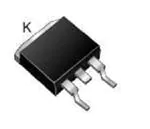
D2PAK (TO-263AB)
• AEC-Q101 qualified
(for ITO-220AC and TO-263AB package)
K
• Material categorization: for definitions of compliance
please see www.vishay.com/doc?99912
2
1
TYPICAL APPLICATIONS
FESB8xT
PIN 1
K
PIN 2
For use in high frequency rectifier of switching mode power
supplies, inverters, freewheeling diodes, DC/DC converters,
and other power switching application.
HEATSINK
DESIGN SUPPORT TOOLS
click logo to get started
MECHANICAL DATA
Case: TO-220AC, ITO-220AC, D2PAK (TO-263AB)
Models
Available
Molding compound meets UL 94V-0 flammability rating
Base P/N-E3 - RoHS-compliant, commercial grade
Base P/NHE3 - RoHS-compliant, AEC-Q101 qualified
PRIMARY CHARACTERISTICS
IF(AV)
8.0 A
VRRM
50 V to 600 V
Terminals: matte tin plated leads, solderable per
J-STD-002 and JESD22-B102
E3 suffix meets JESD 201 class 1A whisker test, HE3 suffix
meets JESD 201 class 2 whisker test
IFSM
125 A
trr
35 ns, 50 ns
VF
0.95 V, 1.30 V, 1.50 V
TJ max.
150 °C
Package
TO-220AC, ITO-220AC, D2PAK (TO-263AB)
Circuit configurations
Single
Polarity: as marked
Mounting Torque: 10 in-lbs max.
MAXIMUM RATINGS (TC = 25 °C unless otherwise noted)
PARAMETER
SYMBOL
FES
8AT
FES
8BT
FES
8CT
FES
8DT
FES
8FT
FES
8GT
FES
8HT
FES
8JT
UNIT
V
Max. repetitive peak reverse voltage
VRRM
50
100
150
200
300
400
500
600
Max. RMS voltage
VRMS
35
70
105
140
210
280
350
420
V
Max. DC blocking voltage
VDC
50
100
150
200
300
400
500
600
V
Max. average forward rectified current
at TC = 100 °C
IF(AV)
8.0
A
Peak forward surge current 8.3 ms single half
sine-wave superimposed on rated load
IFSM
125
A
TJ, TSTG
-55 to +150
°C
VAC
1500
V
Operating storage and temperature range
Isolation voltage (ITO-220AC only)
from terminal to heatsink t = 1 min
Revision: 08-Jun-2018
Document Number: 88600
1
For technical questions within your region: DiodesAmericas@vishay.com, DiodesAsia@vishay.com, DiodesEurope@vishay.com
THIS DOCUMENT IS SUBJECT TO CHANGE WITHOUT NOTICE. THE PRODUCTS DESCRIBED HEREIN AND THIS DOCUMENT
ARE SUBJECT TO SPECIFIC DISCLAIMERS, SET FORTH AT www.vishay.com/doc?91000
�FES8xT, FESF8xT, FESB8xT
www.vishay.com
Vishay General Semiconductor
ELECTRICAL CHARACTERISTICS (TC = 25 °C unless otherwise noted)
PARAMETER
TEST CONDITIONS SYMBOL FES8AT FES8BT FES8CT FES8DT FES8FT FES8GT FES8HT FES8JT UNIT
Max. instantaneous
forward voltage (1)
Max. DC reverse
current at rated DC
blocking voltage
8.0 A
VF
0.95
1.3
TC = 25 °C
1.5
V
10
μA
IR
TC = 100 °C
500
Max. reverse recovery
time
IF = 0.5 A, IR = 1.0
Irr = 0.25 A
trr
Typical junction
capacitance
4.0 V, 1 MHz
CJ
35
50
85
ns
50
pF
Note
(1) Pulse test: 300 μs pulse width, 1 % duty cycle
THERMAL CHARACTERISTICS (TC = 25 °C unless otherwise noted)
PARAMETER
SYMBOL
FES
FESF
FESB
UNIT
RJC
2.2
5.0
2.2
°C/W
Typical thermal resistance from junction to case
ORDERING INFORMATION (Example)
PACKAGE
PREFERRED P/N
UNIT WEIGHT (g)
PACKAGE CODE
BASE QUANTITY
DELIVERY MODE
TO-220AC
FES8JT-E3/45
1.80
45
50/tube
Tube
ITO-220AC
FESF8JT-E3/45
1.85
45
50/tube
Tube
TO-263AB
FESB8JT-E3/45
1.33
45
50/tube
Tube
TO-263AB
FESB8JT-E3/81
1.33
81
800/reel
Tape and reel
ITO-220AC
FESF8JTHE3/45 (1)
1.85
45
50/tube
Tube
TO-263AB
FESB8JTHE3/45 (1)
1.33
45
50/tube
Tube
TO-263AB
FESB8JTHE3/81 (1)
1.33
81
800/reel
Tape and reel
Note
AEC-Q101 qualified, available in ITO-220AC and TO-263AB package
(1)
Revision: 08-Jun-2018
Document Number: 88600
2
For technical questions within your region: DiodesAmericas@vishay.com, DiodesAsia@vishay.com, DiodesEurope@vishay.com
THIS DOCUMENT IS SUBJECT TO CHANGE WITHOUT NOTICE. THE PRODUCTS DESCRIBED HEREIN AND THIS DOCUMENT
ARE SUBJECT TO SPECIFIC DISCLAIMERS, SET FORTH AT www.vishay.com/doc?91000
�FES8xT, FESF8xT, FESB8xT
www.vishay.com
Vishay General Semiconductor
RATINGS AND CHARACTERISTICS CURVES (TC = 25 °C unless otherwise noted)
100
Resistive or Inductive Load
Instantaneous Reverse Leakage
Current (µA)
Average Forward Rectified Current (A)
10
8
Heatsink, Case Temperature, TC
6
Free Air, Ambient Temperature, TA
4
2
10
1
TJ = 100 °C
50 - 200 V
500 - 600 V
0.1
TJ = 25 °C
0.01
0
0
50
100
0
150
40
20
60
80
100
Temperature (°C)
Percent of Rated Peak Reverse Voltage (%)
Fig. 1 - Max. Forward Current Derating Curve
Fig. 4 - Typical Reverse Leakage Characteristics
150
1000
TJ = 25 °C
f = 1.0 MHz
Vsig = 50 mVp-p
TC = 100 °C
8.3 ms Single Half Sine-Wave
125
Junction Capacitance (pF)
Peak Forward Surge Current (A)
TJ = 125 °C
100
75
50
25
100
50 - 200 V
500 - 600 V
0
10
1
10
100
0.1
1
10
Number of Cycles at 60 Hz
Reverse Voltage (V)
Fig. 2 - Max. Non-Repetitive Peak Forward Surge Current
Fig. 5 - Typical Junction Capacitance
100
Instantaneous Forward Current (A)
100
Pulse Width = 300 µs
1 % Duty Cycle
TJ = 125 °C
10
TJ = 25 °C
1
50 - 200 V
300 - 400 V
500 - 600 V
0.1
0.2
0.4
0.6
0.8
1.0
1.2
1.4
1.6
1.8
2.0
Instantaneous Forward Voltage (V)
Fig. 3 - Typical Instantaneous Forward Characteristics
Revision: 08-Jun-2018
Document Number: 88600
3
For technical questions within your region: DiodesAmericas@vishay.com, DiodesAsia@vishay.com, DiodesEurope@vishay.com
THIS DOCUMENT IS SUBJECT TO CHANGE WITHOUT NOTICE. THE PRODUCTS DESCRIBED HEREIN AND THIS DOCUMENT
ARE SUBJECT TO SPECIFIC DISCLAIMERS, SET FORTH AT www.vishay.com/doc?91000
�FES8xT, FESF8xT, FESB8xT
www.vishay.com
Vishay General Semiconductor
PACKAGE OUTLINE DIMENSIONS in inches (millimeters)
TO-220AC
ITO-220AC
0.415 (10.54) MAX.
0.370 (9.40)
0.360 (9.14)
0.154 (3.91) DIA.
0.148 (3.74) DIA.
0.113 (2.87)
0.103 (2.62)
0.076 (1.93) REF.
0.635 (16.13)
0.625 (15.87)
1
PIN
0.603 (15.32)
0.573 (14.55)
0.350 (8.89)
0.330 (8.38)
1
2
0.037 (0.94)
0.027 (0.68)
D2PAK (TO-263AB)
0.411 (10.45)
0.380 (9.65)
0.190 (4.83)
0.160 (4.06)
0.245 (6.22)
MIN.
0.42 (10.66) min.
0.055 (1.40)
0.045 (1.14)
0.33 (8.38) min.
0.360 (9.14)
0.320 (8.13)
K
2
0.624 (15.85)
0.591 (15.00)
0.055 (1.40)
0.047 (1.19)
0.670 (17.02)
0.591 (15.00)
0 to 0.01 (0 to 0.254)
0.110 (2.79)
0.090 (2.29)
0.021 (0.53)
0.014 (0.36)
0.037 (0.940)
0.027 (0.686)
0.105 (2.67)
0.095 (2.41)
0.028 (0.71)
0.020 (0.51)
Mounting Pad Layout
K
1
0.110 (2.79)
0.100 (2.54)
0.035 (0.89)
0.025 (0.64)
0.205 (5.21)
0.195 (4.95)
0.025 (0.64)
0.015 (0.38)
0.022 (0.56)
0.014 (0.36)
0.205 (5.20)
0.195 (4.95)
7° REF.
0.057 (1.45)
0.045 (1.14)
CASE
0.135 (3.43) DIA.
0.122 (3.08) DIA.
7° REF.
0.350 (8.89)
0.330 (8.38)
0.191 (4.85)
0.171 (4.35)
0.560 (14.22)
0.530 (13.46)
0.560 (14.22)
0.530 (13.46)
PIN 1
7° REF.
0.140 (3.56) DIA.
0.125 (3.17) DIA.
0.671 (17.04)
0.651 (16.54)
PIN
0.110 (2.79)
0.100 (2.54)
PIN 2
0.105 (2.67)
0.095 (2.41)
0.600 (15.24)
0.580 (14.73)
1.148 (29.16)
1.118 (28.40)
2
0.160 (4.06)
0.140 (3.56)
0.057 (1.45)
0.045 (1.14)
0.076 (1.93) REF.
45° REF.
0.145 (3.68)
0.135 (3.43)
0.190 (4.83)
0.170 (4.32)
0.110 (2.79)
0.100 (2.54)
0.404 (10.26)
0.384 (9.75)
0.185 (4.70)
0.175 (4.44)
0.055 (1.39)
0.045 (1.14)
0.205 (5.20)
0.195 (4.95)
0.140 (3.56)
0.110 (2.79)
0.15 (3.81) min.
0.08 (2.032) MIN.
0.105 (2.67)
0.095 (2.41)
Revision: 08-Jun-2018
Document Number: 88600
4
For technical questions within your region: DiodesAmericas@vishay.com, DiodesAsia@vishay.com, DiodesEurope@vishay.com
THIS DOCUMENT IS SUBJECT TO CHANGE WITHOUT NOTICE. THE PRODUCTS DESCRIBED HEREIN AND THIS DOCUMENT
ARE SUBJECT TO SPECIFIC DISCLAIMERS, SET FORTH AT www.vishay.com/doc?91000
�