GBUE2560
www.vishay.com
Vishay General Semiconductor
Low VF Single-Phase Single In-Line Bridge Rectifier
FEATURES
• UL recognition file number E312394
• Oxide planar chip junction
• Low forward voltage drop
• Solder dip 275 °C max. 10 s, per JESD 22-B106
• Ideal for printed circuit boards
~
~
+
-
• High surge current capability
-
~
~
+
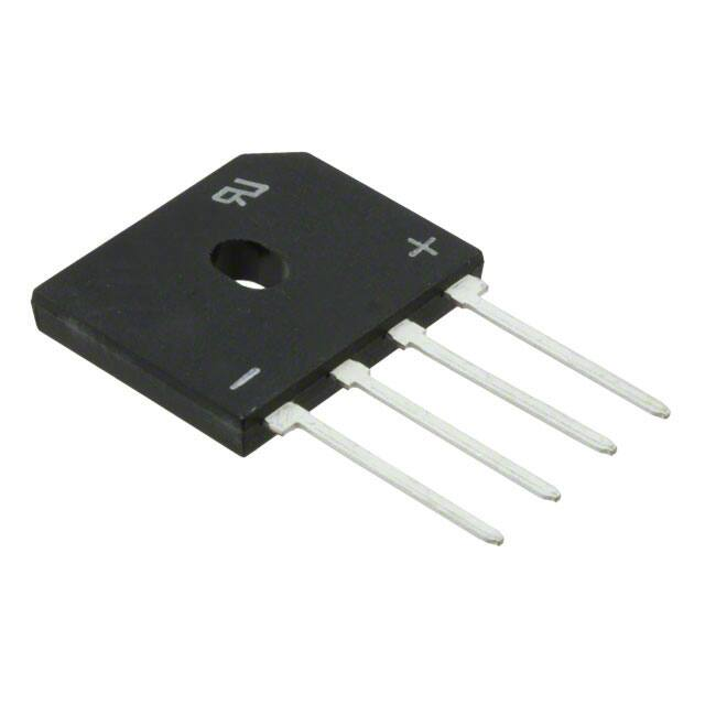
Case Style GBU
• High case dielectric strength of 1500 VRMS
• Material categorization: for definitions of compliance
please see www.vishay.com/doc?99912
Case Style GBU
TYPICAL APPLICATIONS
General purpose use in AC/DC bridge full wave rectification
for switching power supply, home applications, and
white-goods applications specially or telecom power
supply, high efficiency desktop PC and server SMPS.
PRIMARY CHARACTERISTICS
IF(AV)
25 A
VRRM
600 V
IFSM
350 A
VF at IF = 12.5 A (125 °C)
0.75 V
TJ max.
175 °C
Package
GBU
Circuit configuration
In-line
MECHANICAL DATA
Case: GBU
Molding compound meets UL 94 V-0 flammability rating
Base P/N-M3 - halogen-free, RoHS-compliant, and
industrial grade
Terminals: matte tin plated leads, solderable
J-STD-002 and JESD22-B102
M3 suffix meets JESD 201 class 1A whisker test
per
Polarity: as marked on body
Mounting Torque: 10 cm-kg (8.8 inches-lbs) max.
Recommended Torque: 5.7 cm-kg (5 inches-lbs)
MAXIMUM RATINGS (TA = 25 °C unless otherwise noted)
PARAMETER
SYMBOL
Device marking code
GBUE2560
UNIT
GBUE2560
Maximum repetitive peak reverse voltage
VRRM
600
V
Maximum RMS voltage
VRMS
420
V
Maximum DC blocking voltage
VDC
600
V
Maximum average forward rectified output current at
TC = 140 °C
TA = 25 °C
Non-repetitive peak forward surge current
8.3 ms single sine-wave, TJ = 25 °C
Rating for fusing (t < 8.3 ms)
Operating junction and storage temperature range
IO
(1)
25
IO
(2)
4.9
IFSM
350
A
I2t
508
A2s
TJ, TSTG
-55 to +175
°C
A
Notes
(1) Unit case mounted on aIuminum plate heatsink
(2) Units mounted on PCB without heatsink
Revision: 18-Oct-17
Document Number: 87633
1
For technical questions within your region: DiodesAmericas@vishay.com, DiodesAsia@vishay.com, DiodesEurope@vishay.com
THIS DOCUMENT IS SUBJECT TO CHANGE WITHOUT NOTICE. THE PRODUCTS DESCRIBED HEREIN AND THIS DOCUMENT
ARE SUBJECT TO SPECIFIC DISCLAIMERS, SET FORTH AT www.vishay.com/doc?91000
�GBUE2560
www.vishay.com
Vishay General Semiconductor
ELECTRICAL CHARACTERISTICS (TA = 25 °C unless otherwise noted)
PARAMETER
TEST CONDITIONS
Maximum instantaneous forward voltage drop
per diode
IF = 12.5 A
Maximum DC reverse current at rated DC
blocking voltage per diode
VR = 600 V
SYMBOL
TA = 25 °C
VF (1)
TA = 125 °C
TA = 25 °C
IR (2)
TA = 125 °C
TYP.
MAX.
0.88
0.92
0.75
-
0.1
10
27
-
UNIT
V
μA
Typical reverse recovery time
IF = 0.5 A, IR =1.0 A, Irr = 0.25 A
trr
280
-
ns
Typical junction capacitance per diode
4.0 V, 1 MHz
CJ
240
-
pF
Notes
(1) Pulse test: 300 μs pulse width, 1 % duty cycle
(2) Pulse test: Pulse width ≤ 40 ms
THERMAL CHARACTERISTICS (TA = 25 °C unless otherwise noted)
PARAMETER
Typical thermal resistance
SYMBOL
GBUE2560
RθJA (1)
23
RθJC (2)
1.2
UNIT
°C/W
Notes
(1) Without heatsink, free air
(2) With heatsink
ORDERING INFORMATION
PREFERRED P/N
UNIT WEIGHT (g)
PREFERRED PACKAGE CODE
BASE QUANTITY
DELIVERY MODE
GBUE2560-M3/P
3.83
P
20
Tube
30
14.0
25
12.0
Average Power Loss (W)
Average Forward Output Current (A)
RATINGS AND CHARACTERISTICS CURVES (TA = 25 °C unless otherwise noted)
TC measured at device bottom
20
15
10
5
D = 0.5
D = 0.3
10.0
D = 0.8
D = 0.2
D = 0.1
8.0
D = 1.0
6.0
T
4.0
2.0
D = tp/T
tp
10
12
0.0
0
0
25
50
75
100
125
150
175
Case Temperature (°C)
Fig. 1 - Derating Curve Output Rectified Current
0
2
4
6
8
14
Average Forward Current (A)
Fig. 2 - Maximum Non-Repetitive Peak Forward Surge Current
Per Diode
Revision: 18-Oct-17
Document Number: 87633
2
For technical questions within your region: DiodesAmericas@vishay.com, DiodesAsia@vishay.com, DiodesEurope@vishay.com
THIS DOCUMENT IS SUBJECT TO CHANGE WITHOUT NOTICE. THE PRODUCTS DESCRIBED HEREIN AND THIS DOCUMENT
ARE SUBJECT TO SPECIFIC DISCLAIMERS, SET FORTH AT www.vishay.com/doc?91000
�GBUE2560
www.vishay.com
Vishay General Semiconductor
Transient Thermal Impedance (°C/W)
Instantaneous Forward Current (A)
100
TJ = 175 °C
TJ = 125 °C
10
TJ = 100 °C
1
TJ = 75 °C
TJ = 25 °C
0.1
TJ = -40 °C
0.01
0.1 0.2 0.3 0.4 0.5 0.6 0.7 0.8 0.9 1.0 1.1 1.2
Junction to Ambient
10
1
0.1
0.01
0.1
1
10
100
1000
t - Pulse Duration (s)
Fig. 6 - Typical Transient Thermal Impedance Per Diode
1000
400
TJ = 175 °C
Peak Forward Surge Current (A)
Instantaneous Reverse Current (˩A)
Instantaneous Forward Voltage (V)
Fig. 3 - Typical Forward Characteristics Per Diode
100
100
TJ = 125 °C
10
TJ = 100 °C
1
TJ = 75 °C
0.1
TJ = 25 °C
0.01
TJ = -40 °C
0.001
8.3 ms single half sine-wave
300
200
100
0
10
20
30
40
50
60
70
80
90
100
Percent of Rated Peak Reverse Voltage (%)
Fig. 4 - Typical Reverse Leakage Characteristics Per Diode
1
10
100
Number of Cycles at 60 Hz
Fig. 7 - Peak Forward Surge Current
Junction Capacitance (pF)
1000
TJ = 25 °C
f = 1.0 MHz
Vsig = 50 mVp-p
100
10
1
0.1
1
10
100
Reverse Voltage (V)
Fig. 5 - Typical Junction Capacitance Per Diode
Revision: 18-Oct-17
Document Number: 87633
3
For technical questions within your region: DiodesAmericas@vishay.com, DiodesAsia@vishay.com, DiodesEurope@vishay.com
THIS DOCUMENT IS SUBJECT TO CHANGE WITHOUT NOTICE. THE PRODUCTS DESCRIBED HEREIN AND THIS DOCUMENT
ARE SUBJECT TO SPECIFIC DISCLAIMERS, SET FORTH AT www.vishay.com/doc?91000
�GBUE2560
www.vishay.com
Vishay General Semiconductor
PACKAGE OUTLINE DIMENSIONS in inches (millimeters)
GBU
0.020 R (TYP.)
0.310 (7.9)
0.290 (7.4)
0.085 (2.16)
0.065 (1.65)
0.140 (3.56)
0.130 (3.30)
0.880 (22.3)
0.860 (21.8)
0.125 (3.2) x 45°
Chamfer
0.160 (4.1)
0.140 (3.5)
0.075
(1.9) R
.
9° TYP.
0.740 (18.8)
0.720 (18.3)
0.080 (2.03)
0.060 (1.52)
5° TYP.
0.100 (2.54)
0.085 (2.16)
0.080 (2.03)
0.065 (1.65)
0.050 (1.27)
0.040 (1.02)
0.190 (4.83)
0.210 (5.33)
0.710 (18.0)
0.690 (17.5)
0.085 (2.16)
0.075 (1.90)
0.026 (0.66)
0.020 (0.51)
Polarity shown on front side of case, positive lead by beveled corner
Revision: 18-Oct-17
Document Number: 87633
4
For technical questions within your region: DiodesAmericas@vishay.com, DiodesAsia@vishay.com, DiodesEurope@vishay.com
THIS DOCUMENT IS SUBJECT TO CHANGE WITHOUT NOTICE. THE PRODUCTS DESCRIBED HEREIN AND THIS DOCUMENT
ARE SUBJECT TO SPECIFIC DISCLAIMERS, SET FORTH AT www.vishay.com/doc?91000
�Legal Disclaimer Notice
www.vishay.com
Vishay
Disclaimer
ALL PRODUCT, PRODUCT SPECIFICATIONS AND DATA ARE SUBJECT TO CHANGE WITHOUT NOTICE TO IMPROVE
RELIABILITY, FUNCTION OR DESIGN OR OTHERWISE.
Vishay Intertechnology, Inc., its affiliates, agents, and employees, and all persons acting on its or their behalf (collectively,
“Vishay”), disclaim any and all liability for any errors, inaccuracies or incompleteness contained in any datasheet or in any other
disclosure relating to any product.
Vishay makes no warranty, representation or guarantee regarding the suitability of the products for any particular purpose or
the continuing production of any product. To the maximum extent permitted by applicable law, Vishay disclaims (i) any and all
liability arising out of the application or use of any product, (ii) any and all liability, including without limitation special,
consequential or incidental damages, and (iii) any and all implied warranties, including warranties of fitness for particular
purpose, non-infringement and merchantability.
Statements regarding the suitability of products for certain types of applications are based on Vishay’s knowledge of
typical requirements that are often placed on Vishay products in generic applications. Such statements are not binding
statements about the suitability of products for a particular application. It is the customer’s responsibility to validate that a
particular product with the properties described in the product specification is suitable for use in a particular application.
Parameters provided in datasheets and / or specifications may vary in different applications and performance may vary over
time. All operating parameters, including typical parameters, must be validated for each customer application by the customer’s
technical experts. Product specifications do not expand or otherwise modify Vishay’s terms and conditions of purchase,
including but not limited to the warranty expressed therein.
Except as expressly indicated in writing, Vishay products are not designed for use in medical, life-saving, or life-sustaining
applications or for any other application in which the failure of the Vishay product could result in personal injury or death.
Customers using or selling Vishay products not expressly indicated for use in such applications do so at their own risk.
Please contact authorized Vishay personnel to obtain written terms and conditions regarding products designed for
such applications.
No license, express or implied, by estoppel or otherwise, to any intellectual property rights is granted by this document
or by any conduct of Vishay. Product names and markings noted herein may be trademarks of their respective owners.
© 2017 VISHAY INTERTECHNOLOGY, INC. ALL RIGHTS RESERVED
Revision: 08-Feb-17
1
Document Number: 91000
�


 工商网监
湘ICP备2023018690号
工商网监
湘ICP备2023018690号

